- 您现在的位置:买卖IC网 > PDF目录1979 > AD5744RCSUZ-REEL7 (Analog Devices Inc)IC DAC QUAD 14BIT 1LSB 32TQFP PDF资料下载
参数资料
| 型号: | AD5744RCSUZ-REEL7 |
| 厂商: | Analog Devices Inc |
| 文件页数: | 22/32页 |
| 文件大小: | 0K |
| 描述: | IC DAC QUAD 14BIT 1LSB 32TQFP |
| 产品培训模块: | Data Converter Fundamentals DAC Architectures |
| 产品变化通告: | AD5764(R), AD5744R Product Change 04/Sept/2009 |
| 标准包装: | 500 |
| 设置时间: | 10µs |
| 位数: | 14 |
| 数据接口: | 串行 |
| 转换器数目: | 4 |
| 电压电源: | 模拟和数字,双 ± |
| 功率耗散(最大): | 387mW |
| 工作温度: | -40°C ~ 85°C |
| 安装类型: | 表面贴装 |
| 封装/外壳: | 32-TQFP |
| 供应商设备封装: | 32-TQFP(7x7) |
| 包装: | 带卷 (TR) |
| 输出数目和类型: | 4 电压,双极 |
| 采样率(每秒): | * |
第1页第2页第3页第4页第5页第6页第7页第8页第9页第10页第11页第12页第13页第14页第15页第16页第17页第18页第19页第20页第21页当前第22页第23页第24页第25页第26页第27页第28页第29页第30页第31页第32页
Data Sheet
AD5744R
Rev. E | Page 29 of 32
LAYOUT GUIDELINES
In any circuit where accuracy is important, careful considera-
tion of the power supply and ground return layout helps to ensure
the rated performance. Design the PCB on which the AD5744R
is mounted such that the analog and digital sections are separated
and confined to certain areas of the board. If the AD5744R is in
a system where multiple devices require an AGNDx-to-DGND
connection, establish the connection at one point only. Establish
the star ground point as close as possible to the device. The
AD5744R should have ample supply bypassing of 10 μF in parallel
with 0.1 μF on each supply located as close to the package as
possible, ideally right up against the device. The 10 μF capaci-
tors are of the tantalum bead type. The 0.1 μF capacitor should
have low effective series resistance (ESR) and low effective series
inductance (ESI), such as the common ceramic types that
provide a low impedance path to ground at high frequencies to
handle transient currents due to internal logic switching.
The power supply lines of the AD5744R should use as large a
trace as possible to provide low impedance paths and reduce
the effects of glitches on the power supply line. Shield fast-
switching signals, such as clocks with digital ground to avoid
radiating noise to other parts of the board; they should never be
run near the reference inputs. A ground line routed between
the SDIN and SCLK lines helps reduce cross-talk between them.
(A ground line is not required on a multi-layer board because
it has a separate ground plane; however, it is helpful to separate
the lines.) It is essential to minimize noise on the reference inputs
because it couples through to the DAC output. Avoid crossover
of digital and analog signals. Run traces on opposite sides of the
board at right angles to each other to reduce the effects of feed-
through on the board. A microstrip technique is recommended
but not always possible with a double-sided board. In this
technique, the component side of the board is dedicated to the
ground plane, and the signal traces are placed on the solder side.
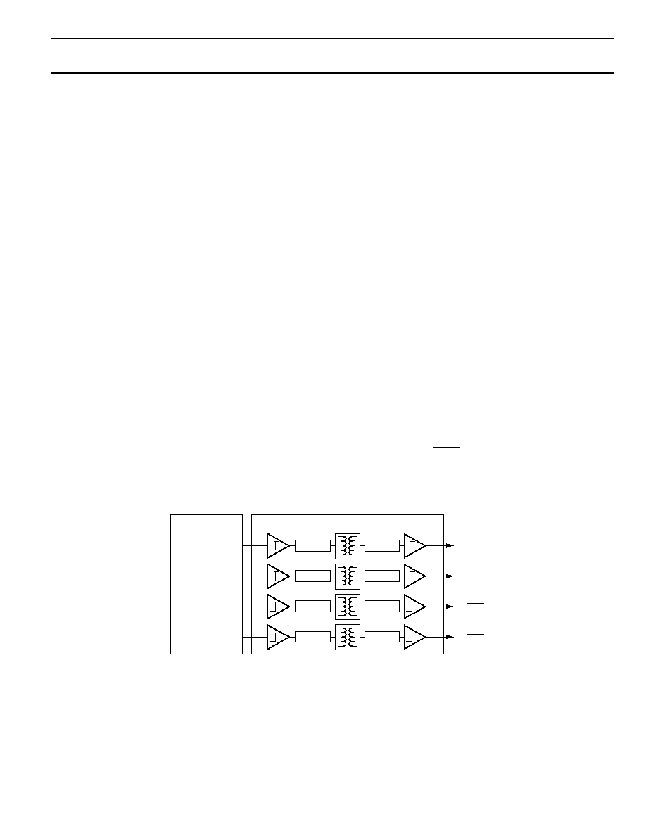
GALVANICALLY ISOLATED INTERFACE
In many process control applications, it is necessary to provide
an isolation barrier between the controller and the unit being
controlled to protect and isolate the controlling circuitry from
any hazardous common-mode voltages that may occur. Isocou-
plers provide voltage isolation in excess of 2.5 kV. The serial
loading structure of the AD5744R makes it ideal for isolated
interfaces because the number of interface lines is kept to a min-
imum. Figure 44 shows a 4-channel isolated interface to the
AD5744R using an ADuM1400 iCoupler product. For more
information on iCoupler products, refer to www.analog.com.
MICROPROCESSOR INTERFACING
Microprocessor interfacing to the AD5744R is accomplished
using a serial bus that uses standard protocol that is compatible
with microcontrollers and DSP processors. The communications
channel is a 3-wire (minimum) interface consisting of a clock
signal, a data signal, and a synchronization signal. The AD5744R
requires a 24-bit data-word with data valid on the falling edge
of SCLK.
For all the interfaces, a DAC output update can be performed
automatically when all the data is clocked in, or it can be done
under the control of LDAC. The contents of the data register
can be read using the readback function.
VIA
SERIAL CLOCK OUT
TO SCLK
VOA
ENCODE
DECODE
VIB
SERIAL DATA OUT
TO SDIN
VOB
ENCODE
DECODE
VIC
SYNC OUT
TO SYNC
VOC
ENCODE
DECODE
VID
CONTROL OUT
TO LDAC
VOD
ENCODE
DECODE
MICROCONTROLLER
ADuM1400*
*ADDITIONAL PINS OMITTED FOR CLARITY.
06
5-
0
6
5
Figure 44. Isolated Interface
相关PDF资料 |
PDF描述 |
|---|---|
| AD574AKPZ-REEL | IC ADC 12BIT W/REF/CLK 28-PLCC |
| AD5752AREZ | IC DAC DUAL 16BIT SERIAL 24TSSOP |
| AD5752RBREZ-REEL7 | IC DAC DUAL 16BIT SERIAL 24TSSOP |
| AD5754BREZ-REEL7 | IC DAC 16BIT DSP/SRL 24TSSOP |
| AD5755-1ACPZ | IC DAC 16BIT SERIAL 64LFCSP |
相关代理商/技术参数 |
参数描述 |
|---|---|
| AD5748 | 制造商:AD 制造商全称:Analog Devices 功能描述:Industrial Current/Voltage Output Driver with Programmable Ranges |
| AD5748_1 | 制造商:AD 制造商全称:Analog Devices 功能描述:Industrial Current/Voltage Output Driver with Programmable Ranges |
| AD5748ACPZ | 功能描述:IC I/V OUTPUT DRIVER 32LFCSP RoHS:是 类别:集成电路 (IC) >> Linear - Amplifiers - Instrumentation 系列:- 标准包装:73 系列:Over-The-Top® 放大器类型:通用 电路数:4 输出类型:满摆幅 转换速率:0.07 V/µs 增益带宽积:200kHz -3db带宽:- 电流 - 输入偏压:1nA 电压 - 输入偏移:285µV 电流 - 电源:50µA 电流 - 输出 / 通道:25mA 电压 - 电源,单路/双路(±):2 V ~ 44 V,±1 V ~ 22 V 工作温度:-40°C ~ 85°C 安装类型:表面贴装 封装/外壳:16-WFDFN 裸露焊盘 供应商设备封装:16-DFN-EP(5x3) 包装:管件 |
| AD5748ACPZ-RL7 | 功能描述:IC I/V OUTPUT DRIVER 32LFCSP RoHS:是 类别:集成电路 (IC) >> Linear - Amplifiers - Instrumentation 系列:- 产品培训模块:Lead (SnPb) Finish for COTS Obsolescence Mitigation Program 标准包装:1 系列:- 放大器类型:电流检测 电路数:1 输出类型:- 转换速率:- 增益带宽积:125kHz -3db带宽:- 电流 - 输入偏压:- 电压 - 输入偏移:100µV 电流 - 电源:1.1µA 电流 - 输出 / 通道:- 电压 - 电源,单路/双路(±):- 工作温度:-40°C ~ 85°C 安装类型:表面贴装 封装/外壳:4-WFBGA,CSPBGA 供应商设备封装:4-UCSP(2x2) 包装:剪切带 (CT) 其它名称:MAX9634WERS+TCT |
| AD5749 | 制造商:AD 制造商全称:Analog Devices 功能描述:Industrial Current Out Driver, Single-Supply, 55 V Maximum Supply, Programmable Ranges |
发布紧急采购,3分钟左右您将得到回复。