- 您现在的位置:买卖IC网 > PDF目录373890 > AD6624A (Analog Devices, Inc.) Four-Channel, 100 MSPS Digital Receive Signal Processor (RSP) PDF资料下载
参数资料
| 型号: | AD6624A |
| 厂商: | Analog Devices, Inc. |
| 英文描述: | Four-Channel, 100 MSPS Digital Receive Signal Processor (RSP) |
| 中文描述: | 四通道,100 MSPS的数字接收信号处理器(RSP) |
| 文件页数: | 25/40页 |
| 文件大小: | 636K |
| 代理商: | AD6624A |
第1页第2页第3页第4页第5页第6页第7页第8页第9页第10页第11页第12页第13页第14页第15页第16页第17页第18页第19页第20页第21页第22页第23页第24页当前第25页第26页第27页第28页第29页第30页第31页第32页第33页第34页第35页第36页第37页第38页第39页第40页
REV. 0
AD6624A
–25–
24
16
12
I[23:12]
I[1:8]
QI[1:8]
I[7:0]
Q[23:2]
ZQ[7:0]
SCLK
SDFS
SDFE
SDO
1 2 3 4 5 6 7 8 9101 2 3 4 5 6 7 8 9201 2 3 4 5 6 7 8 9301 2 3 4 5 6 7 8 9401 2 3 4 5 6 7 8 9
Figure 29. SDFS Valid for One SCLK Cycle
24
16
12
I[23:12]
I[23:13]
I[1:8]
Q[23:20]
I[7:0]
Q[23:2]
Q[23:2]
Q[11:8]
Q[7:0]
Z, NEW-I
SCLK
SDFS
SDFE
SDO
1 2 3 4 5 6 7 8 9101 2 3 4 5 6 7 8 9201 2 3 4 5 6 7 8 9301 2 3 4 5 6 7 8 9401 2 3 4 5 6 7 8 9
Figure 30. SDFS Is High During Data Shift
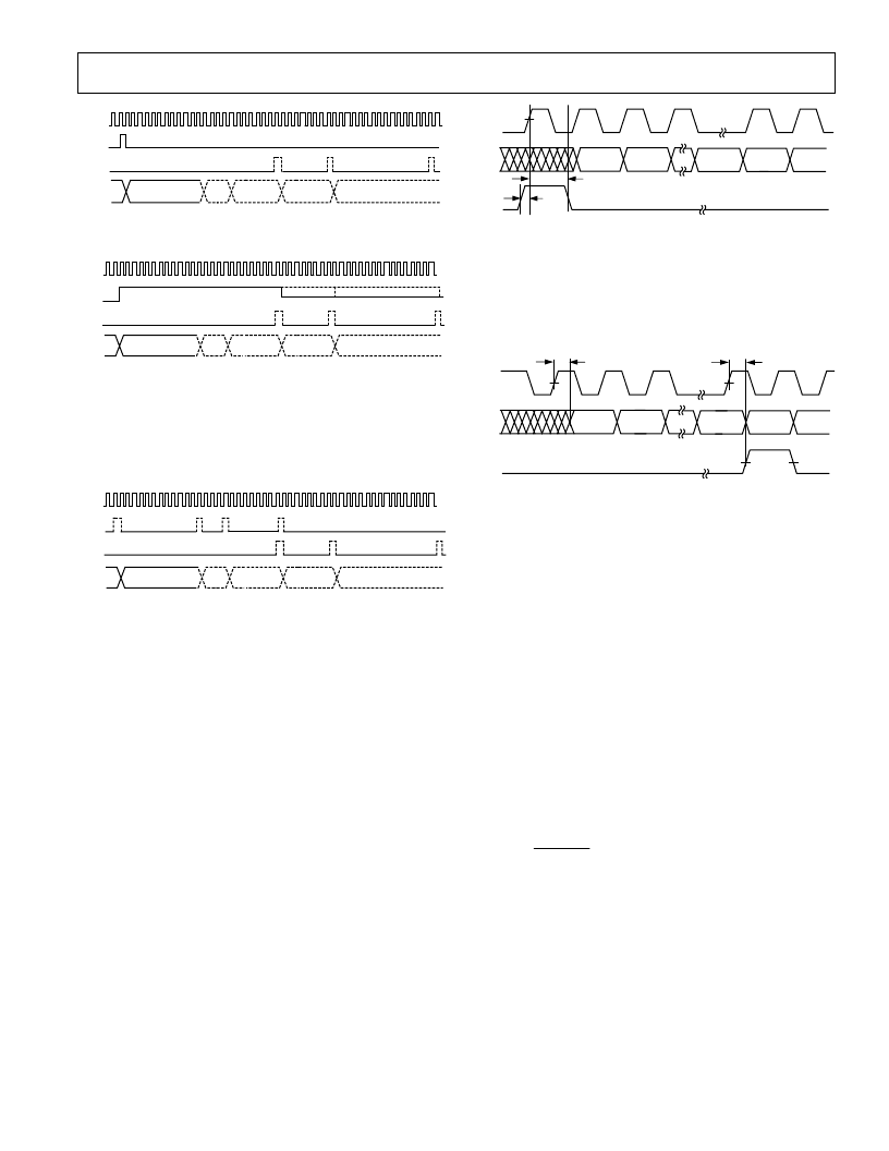
In the final mode, the SDFS bit goes high as in the first mode,
one clock cycle prior to the actual data. However, a second SDFS
is inserted one clock cycle prior to the shift of the first Q bit. In
this manner, each word out of the AD6624A is accompanied by
an SDFS.
SCLK
1 2 3 4 5 6 7 8 9101 2 3 4 5 6 7 8 9201 2 3 4 5 6 7 8 9301 2 3 4 5 6 7 8 9401 2 3 4 5 6 7 8 9
SDFS
SDFE
SDO
24
16
12
I[23:12]
I[23:12]
I[1:8]
Q[23:20]
I[7:0]
Q[19:8]
Q[23:2]
Z, NEW-I
ZQ[7:0]
Z, NEW-I
Figure 31. A Second SDFS Inserted Prior to First Q Bit
Regardless of the mode above, the SDFE behaves the same in
each. On the last bit of the serial frame (least significant bit of
the Q word), the Serial Data Frame End (SDFE) is raised. The
SDFE signal can either be used by the DSP to indicate the end
of the frame or it can be used as the SDFS (Serial Data Frame
Sync) of another AD6624A chip or channel running in Serial
Cascade mode.
Serial Data Frame (Serial Cascade)
Any of the AD6624A serial outputs may be operated in the
serial cascade mode (serial slave). In this mode, the selected
AD6624A channel requires an external device such as a DSP to
issue the serial clock and SDFS.
To operate successfully in the serial cascade mode, the DSP
must have some indication that the AD6624A channel
’
s serial
buffer is ready to send data. This is indicated by the assertion of
the DRx pin where
“
x
”
is the channel number. This pin should
be tied to an interrupt or flag pin of the DSP. In this manner,
the DSP will know when to service the serial port.
When the DSP begins handling the serial service, the serial port
should be configured such that the SDFS pin is asserted one
clock cycle prior to shifting data. As such, the AD6624A channel
samples the SDFS pin on the rising edge of the serial clock. On
the next rising edge of the serial clock, the AD6624A serial
port begins shifting data until the specified number of bits
has been shifted.
SCLK
SDO
SDFS
I
15
I
14
Q
1
Q
0
t
HSF
t
SSF
Figure 32. SDO, SDFS Switching Characteristics (SBM = 0)
On the last bit of the serial frame (least significant bit of the Q
word), the SDFE is raised. The SDFE signal can either be used
by the DSP to indicate the end of the frame or it can be used as
the SDFS of another AD6624A chip or channel running in Serial
Cascade mode.
SCLK
SDO
SDFE
t
DSDFE
I
15
I
14
Q
1
Q
0
t
DSO
Figure 33. SDO, SDFE Switching Characteristics
Configuring the Serial Ports
Each Serial Output Port may function as either a master or
slave. A Serial Bus Master will provide SCLK (SCLK0, SCLK1,
SCLK2, SCLK3) and SDFS outputs. A Serial Slave will accept
these signals as inputs. Upon the lift of
RESET
, Serial Port 0
will become a master if the SBM0 pin is high, and a slave if
SBM0 is low. Serial Ports 1, 2, and 3 will always default to serial
slaves when
RESET
is taken low. They can be programmed as a
master by setting the SBM1, SBM2, and SBM3 bits in the
0xA9
Registers high.
Serial Port Data Rate
If a Serial Port is defined as a master, the SCLK frequency is
defined by Equation 15. f
CLK
is the frequency of the master
clock of the AD6624A channel and SDIV is the Serial Divi-
sion word for the channel (1, 2, or 3). The SDIV for Serial
Port 0 is located directly as pins on the package for easy hard-
ware configuration and is
not
mapped into 0xA9. For Serial
Ports 1, 2, and 3, the internal register 0xA9 Bits 3
–
0 define the
SDIV (SDIV0, SDIV1, SDIV2, SDIV3) word.
f
f
SDIV
SCLK
CLK
=
+
1
(16)
Serial Port to DSP Interconnection
The AD6624A is very flexible in the manner that the serial ports
can be configured and connected to external devices. Each of
the channels can be independently configured and processed by
different DSPs or all of the channels can be chained together to
form a TDM (time division multiplexed) serial chain. This allows
one DSP to handle all of the channels. Additionally, the channels
can be parceled off in any combination in between.
相关PDF资料 |
PDF描述 |
|---|---|
| AD6624AABC | Four-Channel, 100 MSPS Digital Receive Signal Processor (RSP) |
| AD6630AR-REEL | Differential, Low Noise IF Gain Block with Output Clamping |
| AD6630AR | Differential, Low Noise IF Gain Block with Output Clamping |
| AD6630PCB | Differential, Low Noise IF Gain Block with Output Clamping |
| AD6630R | Differential, Low Noise IF Gain Block with Output Clamping |
相关代理商/技术参数 |
参数描述 |
|---|---|
| AD6624AABC | 制造商:Advanced Micro Devices 功能描述: |
| AD6624AABCZ | 功能描述:DIGITAL SIGNAL PROC 196 CSP-BGA RoHS:是 类别:集成电路 (IC) >> 专用 IC 系列:* 产品培训模块:Lead (SnPb) Finish for COTS Obsolescence Mitigation Program 标准包装:1 系列:- 类型:调帧器 应用:数据传输 安装类型:表面贴装 封装/外壳:400-BBGA 供应商设备封装:400-PBGA(27x27) 包装:散装 |
| AD6624AS | 制造商:AD 制造商全称:Analog Devices 功能描述:Four-Channel, 80 MSPS Digital Receive Signal Processor (RSP) |
| AD6624AS/PCB | 制造商:AD 制造商全称:Analog Devices 功能描述:Four-Channel, 100 MSPS Digital Receive Signal Processor (RSP) |
| AD6624S/PCB | 制造商:AD 制造商全称:Analog Devices 功能描述:Four-Channel, 80 MSPS Digital Receive Signal Processor (RSP) |
发布紧急采购,3分钟左右您将得到回复。