- 您现在的位置:买卖IC网 > PDF目录1980 > AD7190BRUZ-REEL (Analog Devices Inc)IC ADC 2CH 24BIT W/PGA 24TSSOP PDF资料下载
参数资料
| 型号: | AD7190BRUZ-REEL |
| 厂商: | Analog Devices Inc |
| 文件页数: | 24/41页 |
| 文件大小: | 0K |
| 描述: | IC ADC 2CH 24BIT W/PGA 24TSSOP |
| 设计资源: | Precision Weigh Scale Design Using AD7190 with Internal PGA (CN0102) |
| 标准包装: | 2,500 |
| 位数: | 24 |
| 采样率(每秒): | 4.8k |
| 数据接口: | DSP,MICROWIRE?,QSPI?,串行,SPI? |
| 转换器数目: | 1 |
| 电压电源: | 模拟和数字 |
| 工作温度: | -40°C ~ 105°C |
| 安装类型: | 表面贴装 |
| 封装/外壳: | 24-TSSOP(0.173",4.40mm 宽) |
| 供应商设备封装: | 24-TSSOP |
| 包装: | 带卷 (TR) |
| 输入数目和类型: | 2 个差分,双极;4 个伪差分,双极 |
第1页第2页第3页第4页第5页第6页第7页第8页第9页第10页第11页第12页第13页第14页第15页第16页第17页第18页第19页第20页第21页第22页第23页当前第24页第25页第26页第27页第28页第29页第30页第31页第32页第33页第34页第35页第36页第37页第38页第39页第40页第41页
Data Sheet
AD7190
Rev. C | Page 29 of 40
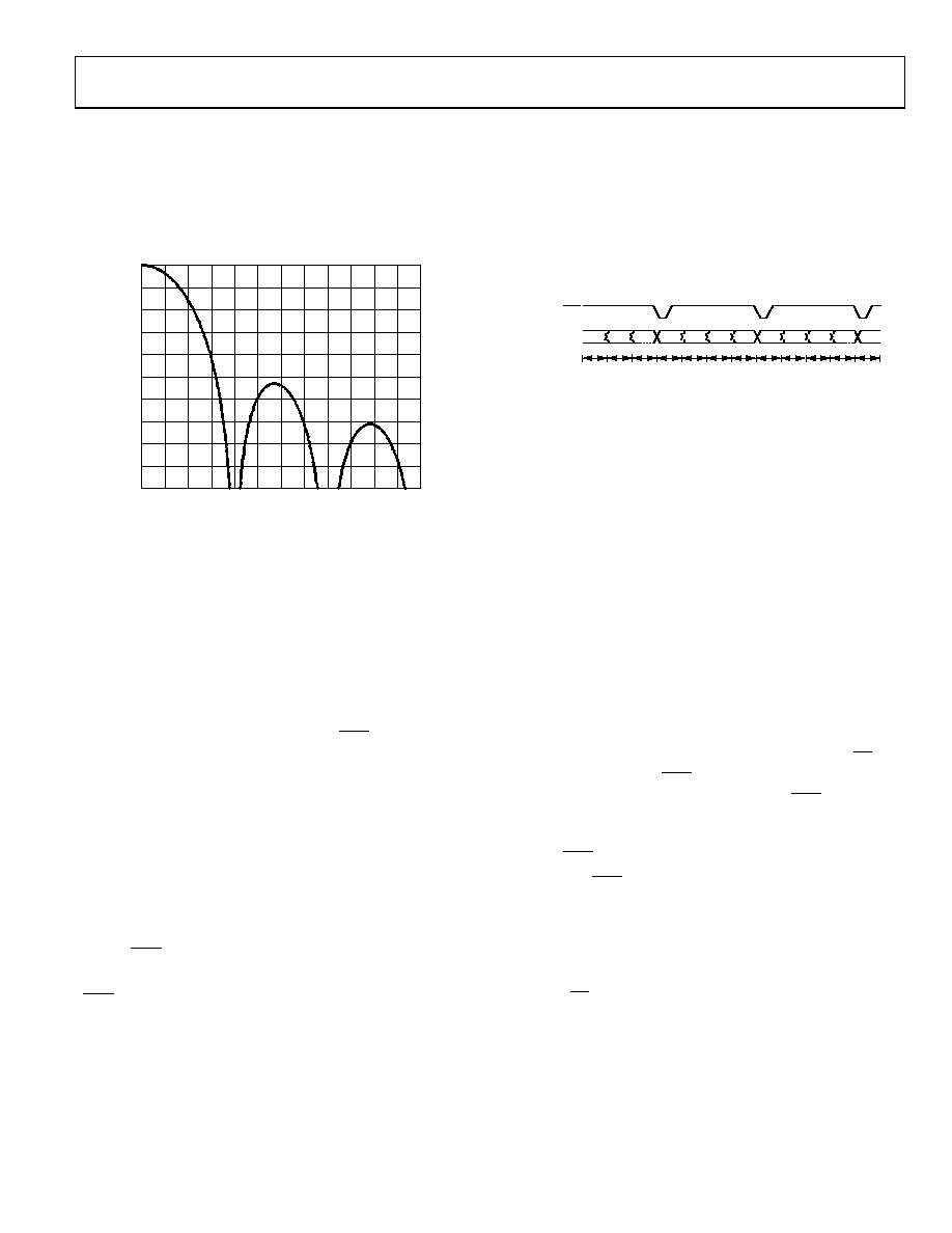
is 50 Hz (sinc4 filter); 50 Hz rejection is no longer achieved. The
ADC needs to operate with an output data rate of 12.5 Hz to
obtain 50 Hz rejection when zero latency is enabled. To obtain
simultaneous 50 Hz/60 Hz rejection, the REJ60 bit in the mode
register can be set when the output data rate is equal to 12.5 Hz.
The stop-band attenuation is considerably reduced also (3 dB
compared with 53 dB in the nonzero latency mode).
0
–10
–20
–30
–40
–50
–60
–70
–80
–90
–100
0
100
50
200
300
400
500
150
250
350
450
550 600
FILTE
R
GA
IN
(
dB
)
FREQUENCY (Hz)
07640-
020
Figure 27. Sinc4 Filter Response (50 Hz Output Data Rate, Zero Latency)
Channel Sequencer
The AD7190 includes a channel sequencer, which simplifies
communications with the device in multichannel applications.
The sequencer also optimizes the channel throughput of the
device as the sequencer switches channels at the optimum rate
rather than waiting for instructions via the SPI interface.
Bits CH0 to Bit CH7 in the configuration register are used to
enable the required channels. In continuous conversion mode,
the ADC selects each of the enabled channels in sequence and
performs a conversion on the channel. The RDY pin goes low
when a valid conversion is available on each channel. When
several channels are enabled, the contents of the status register
should be attached to the 24-bit word so that the user can
identify the channel that corresponds to each conversion. To
attach the status register value to the conversion, Bit DAT_STA
in the mode register should be set to 1.
When several channels are enabled, the ADC must allow the
complete settling time to generate a valid conversion each time
that the channel is changed. The AD7190 takes care of this:
when a channel is selected, the modulator and filter are reset
and the RDY pin is taken high. The AD7190 then allows the
complete settling time to generate the first conversion.
RDY only goes low when a valid conversion is available. The
AD7190 then selects the next enabled channel and converts on
that channel. The user can then read the data register while the
ADC is performing the conversion on the next channel.
The time required to read a valid conversion from all enabled
channels is equal to
tSETTLE × Number of Enabled Channels
For example, if the sinc4 filter is selected, chop is disabled and
zero latency is disabled, conversions are available at 1/fADC when
converting on a single channel, where fADC is equal to the output
data rate. The settling time is equal to
tSETTLE = 4/fADC
The time required to sample N channels is
4/(fADC × N)
RDY
CONVERSIONS
CHANNEL A
CHANNEL B
1/fADC
CHANNEL C
07640-
019
Figure 28. Channel Sequencer
DIGITAL INTERFACE
As indicated in the On-Chip Registers section, the programmable
functions of the AD7190 are controlled using a set of on-chip
registers. Data is written to these registers via the serial interface
of the part. Read access to the on-chip registers is also provided
by this interface. All communication with the part must start with
a write to the communications register. After power-on or reset,
the device expects a write to its communications register. The data
written to this register determines whether the next operation is a
read operation or a write operation and also determines which
register this read or write operation affects. Therefore, write
access to any of the other registers on the part begins with a write
operation to the communications register, followed by a write to
the selected register. A read operation from any other register
(except when continuous read mode is selected) starts with a write
to the communications register, followed by a read operation from
the selected register.
The serial interface of the AD7190 consists of four signals: CS,
DIN, SCLK, and DOUT/RDY. The DIN line is used to transfer
data into the on-chip registers, whereas DOUT/RDY is used for
accessing data from the on-chip registers. SCLK is the serial clock
input for the device, and all data transfers (either on DIN or
DOUT/RDY) occur with respect to the SCLK signal.
The DOUT/ RDY pin functions as a data ready signal also, the
line going low when a new data-word is available in the output
register. It is reset high when a read operation from the data
register is complete. It also goes high prior to the updating of the
data register to indicate when not to read from the device, to
ensure that a data read is not attempted while the register is being
updated. CS is used to select a device. It can be used to decode the
AD7190 in systems where several components are connected to
the serial bus.
相关PDF资料 |
PDF描述 |
|---|---|
| AD7191BRUZ | IC ADC 2CH 24B SD 24TSSOP |
| AD7192BRUZ | IC ADC 24BIT 2CH W/PGA 24-TSSOP |
| AD7193BCPZ | IC ADC 24BIT SPI 4.8KHZ 32LFCSP |
| AD7194BCPZ | IC ADC 24BIT SPI 4.8K 32-LFCSP |
| AD7195BCPZ-RL7 | IC AFE 24BIT 4.8K 32LFSP |
相关代理商/技术参数 |
参数描述 |
|---|---|
| AD7190WBRUZ | 功能描述:24 Bit Analog to Digital Converter 2, 4 Input 1 Sigma-Delta 24-TSSOP 制造商:analog devices inc. 系列:- 包装:管件 零件状态:有效 位数:24 采样率(每秒):4.8k 输入数:2,4 输入类型:差分,个伪差分 数据接口:SPI,DSP 配置:MUX-PGA-ADC 无线电 - S/H:ADC:- A/D 转换器数:1 架构:三角积分 参考类型:外部, 内部 电压 - 电源,模拟:5V 电压 - 电源,数字:2.7 V ~ 5.25 V 特性:PGA,温度传感器 工作温度:-40°C ~ 105°C 封装/外壳:24-TSSOP(0.173",4.40mm 宽) 供应商器件封装:24-TSSOP 标准包装:1 |
| AD7190WBRUZ-RL | 制造商:Analog Devices 功能描述: |
| AD7191 | 制造商:AD 制造商全称:Analog Devices 功能描述:Pin-Programmable, Ultralow Noise, 24-Bit, Sigma-Delta ADC for Bridge Sensors |
| AD7191A/0B | 制造商:Sony Nec Optiarc America 功能描述:DOUBLE DUAL INTERNAL DVDRW PATA BEZEL 20X/18X12XRAM - Bulk |
| AD7191BRUZ | 功能描述:IC ADC 2CH 24B SD 24TSSOP RoHS:是 类别:集成电路 (IC) >> 数据采集 - 模数转换器 系列:- 标准包装:1,000 系列:- 位数:16 采样率(每秒):45k 数据接口:串行 转换器数目:2 功率耗散(最大):315mW 电压电源:模拟和数字 工作温度:0°C ~ 70°C 安装类型:表面贴装 封装/外壳:28-SOIC(0.295",7.50mm 宽) 供应商设备封装:28-SOIC W 包装:带卷 (TR) 输入数目和类型:2 个单端,单极 |
发布紧急采购,3分钟左右您将得到回复。