- 您现在的位置:买卖IC网 > PDF目录1980 > AD7190BRUZ-REEL (Analog Devices Inc)IC ADC 2CH 24BIT W/PGA 24TSSOP PDF资料下载
参数资料
| 型号: | AD7190BRUZ-REEL |
| 厂商: | Analog Devices Inc |
| 文件页数: | 3/41页 |
| 文件大小: | 0K |
| 描述: | IC ADC 2CH 24BIT W/PGA 24TSSOP |
| 设计资源: | Precision Weigh Scale Design Using AD7190 with Internal PGA (CN0102) |
| 标准包装: | 2,500 |
| 位数: | 24 |
| 采样率(每秒): | 4.8k |
| 数据接口: | DSP,MICROWIRE?,QSPI?,串行,SPI? |
| 转换器数目: | 1 |
| 电压电源: | 模拟和数字 |
| 工作温度: | -40°C ~ 105°C |
| 安装类型: | 表面贴装 |
| 封装/外壳: | 24-TSSOP(0.173",4.40mm 宽) |
| 供应商设备封装: | 24-TSSOP |
| 包装: | 带卷 (TR) |
| 输入数目和类型: | 2 个差分,双极;4 个伪差分,双极 |
第1页第2页当前第3页第4页第5页第6页第7页第8页第9页第10页第11页第12页第13页第14页第15页第16页第17页第18页第19页第20页第21页第22页第23页第24页第25页第26页第27页第28页第29页第30页第31页第32页第33页第34页第35页第36页第37页第38页第39页第40页第41页
AD7190
Data Sheet
Rev. C | Page 10 of 40
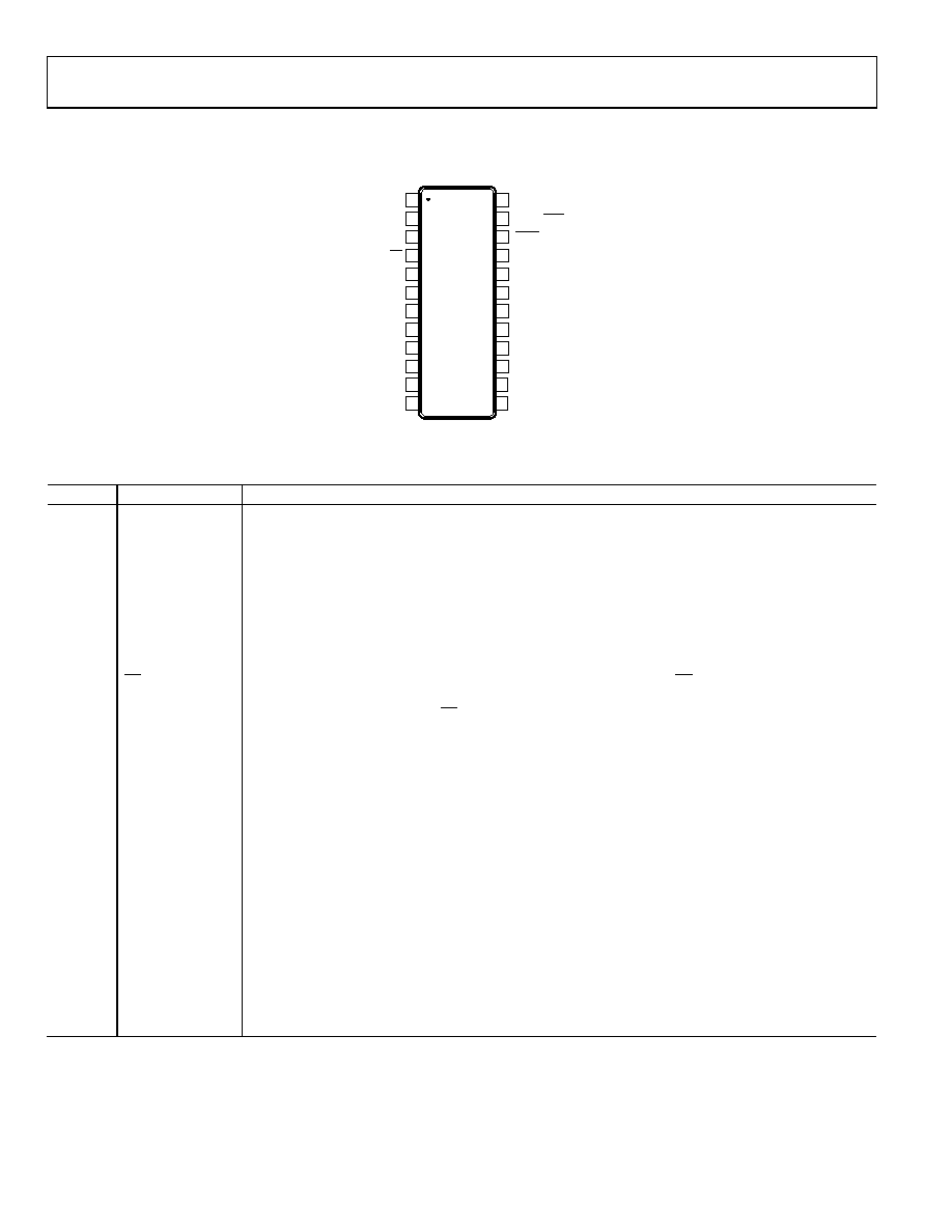
PIN CONFIGURATION AND FUNCTION DESCRIPTIONS
NC = NO CONNECT
1
2
3
4
5
6
7
8
9
10
12
11
MCLK2
SCLK
CS
P1/REFIN2(+)
P2
P3
MCLK1
P0/REFIN2(–)
NC
AINCOM
AIN2
AIN1
20
21
22
23
24
19
18
17
16
15
14
13
DOUT/RDY
SYNC
DVDD
AGND
DGND
AVDD
BPDSW
REFIN1(–)
AIN3
AIN4
REFIN1(+)
DIN
AD7190
TOP VIEW
(Not to Scale)
07640-
005
Figure 5. Pin Configuration
Table 5. Pin Function Descriptions
Pin No.
Mnemonic
Description
1
MCLK1
When the master clock for the device is provided externally by a crystal, the crystal is connected between
MCLK1 and MCLK2.
2
MCLK2
Master Clock Signal for the Device. The AD7190 has an internal 4.92 MHz clock. This internal clock can be
made available on the MCLK2 pin. The clock for the AD7190 can be provided externally also in the form of
a crystal or external clock. A crystal can be tied across the MCLK1 and MCLK2 pins. Alternatively, the
MCLK2 pin can be driven with a CMOS-compatible clock and the MCLK1 pin left unconnected.
3
SCLK
Serial Clock Input. This serial clock input is for data transfers to and from the ADC. The SCLK has a Schmitt-
triggered input, making the interface suitable for opto-isolated applications. The serial clock can be
continuous with all data transmitted in a continuous train of pulses. Alternatively, it can be a noncon-
tinuous clock with the information transmitted to or from the ADC in smaller batches of data.
4
CS
Chip Select Input. This is an active low logic input used to select the ADC. CS can be used to select the ADC
in systems with more than one device on the serial bus or as a frame synchronization signal in
communicating with the device. CS can be hardwired low, allowing the ADC to operate in 3-wire mode
with SCLK, DIN, and DOUT used to interface with the device.
5
P3
Digital Output Pin. This pin can function as a general-purpose output bit referenced between AVDD and AGND.
6
P2
Digital Output Pin. This pin can function as a general-purpose output bit referenced between AVDD and AGND.
7
P1/REFIN2(+)
Digital Output Pin/Positive Reference Input. This pin functions as a general-purpose output bit referenced
between AVDD and AGND. When REFSEL = 1, this pin functions as REFIN2(+). An external reference can be
applied between REFIN2(+) and REFIN2(). REFIN2(+) can lie anywhere between AVDD and AGND + 1 V. The
nominal reference voltage, (REFIN2(+) REFIN2()), is AVDD, but the part functions with a reference from
1 V to AVDD.
8
P0/REFIN2()
Digital Output Pin/Negative Reference Input. This pin functions as a general-purpose output bit referenced
between AVDD and AGND. When REFSEL = 1, this pin functions as REFIN2(). This reference input can lie
anywhere between AGND and AVDD 1 V.
9
NC
No Connect. This pin should be tied to AGND.
10
AINCOM
Analog Input AIN1 to Analog Input AIN4 are referenced to this input when configured for pseudo
differential operation.
11
AIN1
Analog Input. It can be configured as the positive input of a fully differential input pair when used with
AIN2 or as a pseudo differential input when used with AINCOM.
12
AIN2
Analog Input. It can be configured as the negative input of a fully differential input pair when used with
AIN1 or as a pseudo differential input when used with AINCOM.
相关PDF资料 |
PDF描述 |
|---|---|
| AD7191BRUZ | IC ADC 2CH 24B SD 24TSSOP |
| AD7192BRUZ | IC ADC 24BIT 2CH W/PGA 24-TSSOP |
| AD7193BCPZ | IC ADC 24BIT SPI 4.8KHZ 32LFCSP |
| AD7194BCPZ | IC ADC 24BIT SPI 4.8K 32-LFCSP |
| AD7195BCPZ-RL7 | IC AFE 24BIT 4.8K 32LFSP |
相关代理商/技术参数 |
参数描述 |
|---|---|
| AD7190WBRUZ | 功能描述:24 Bit Analog to Digital Converter 2, 4 Input 1 Sigma-Delta 24-TSSOP 制造商:analog devices inc. 系列:- 包装:管件 零件状态:有效 位数:24 采样率(每秒):4.8k 输入数:2,4 输入类型:差分,个伪差分 数据接口:SPI,DSP 配置:MUX-PGA-ADC 无线电 - S/H:ADC:- A/D 转换器数:1 架构:三角积分 参考类型:外部, 内部 电压 - 电源,模拟:5V 电压 - 电源,数字:2.7 V ~ 5.25 V 特性:PGA,温度传感器 工作温度:-40°C ~ 105°C 封装/外壳:24-TSSOP(0.173",4.40mm 宽) 供应商器件封装:24-TSSOP 标准包装:1 |
| AD7190WBRUZ-RL | 制造商:Analog Devices 功能描述: |
| AD7191 | 制造商:AD 制造商全称:Analog Devices 功能描述:Pin-Programmable, Ultralow Noise, 24-Bit, Sigma-Delta ADC for Bridge Sensors |
| AD7191A/0B | 制造商:Sony Nec Optiarc America 功能描述:DOUBLE DUAL INTERNAL DVDRW PATA BEZEL 20X/18X12XRAM - Bulk |
| AD7191BRUZ | 功能描述:IC ADC 2CH 24B SD 24TSSOP RoHS:是 类别:集成电路 (IC) >> 数据采集 - 模数转换器 系列:- 标准包装:1,000 系列:- 位数:16 采样率(每秒):45k 数据接口:串行 转换器数目:2 功率耗散(最大):315mW 电压电源:模拟和数字 工作温度:0°C ~ 70°C 安装类型:表面贴装 封装/外壳:28-SOIC(0.295",7.50mm 宽) 供应商设备封装:28-SOIC W 包装:带卷 (TR) 输入数目和类型:2 个单端,单极 |
发布紧急采购,3分钟左右您将得到回复。