- 您现在的位置:买卖IC网 > PDF目录10182 > AD7851KRZ (Analog Devices Inc)IC ADC 14BIT SRL 333KSPS 24-SOIC PDF资料下载
参数资料
| 型号: | AD7851KRZ |
| 厂商: | Analog Devices Inc |
| 文件页数: | 19/36页 |
| 文件大小: | 0K |
| 描述: | IC ADC 14BIT SRL 333KSPS 24-SOIC |
| 标准包装: | 31 |
| 位数: | 14 |
| 采样率(每秒): | 333k |
| 数据接口: | 8051,QSPI?,串行,SPI? µP |
| 转换器数目: | 2 |
| 功率耗散(最大): | 89.25mW |
| 电压电源: | 模拟和数字 |
| 工作温度: | 0°C ~ 85°C |
| 安装类型: | 表面贴装 |
| 封装/外壳: | 24-SOIC(0.295",7.50mm 宽) |
| 供应商设备封装: | 24-SOIC W |
| 包装: | 管件 |
| 输入数目和类型: | 1 个伪差分,单极;1 个伪差分,双极 |
第1页第2页第3页第4页第5页第6页第7页第8页第9页第10页第11页第12页第13页第14页第15页第16页第17页第18页当前第19页第20页第21页第22页第23页第24页第25页第26页第27页第28页第29页第30页第31页第32页第33页第34页第35页第36页
AD7851
–26–
REV. B
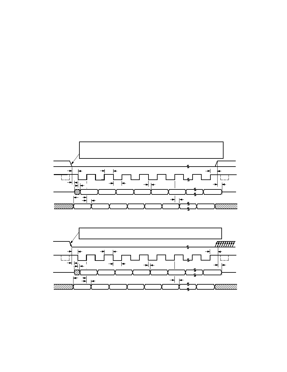
Mode 2 (3-Wire SPI/QSPI Interface Mode)
Default Interface Mode
Figure 35 shows the timing diagram for Interface Mode 2 which
is the SPI/QSPI interface mode. Here the
SYNC input is active
low and may be pulsed or tied permanently low. If
SYNC is
permanently low, 16 clock pulses must be applied to the SCLK
pin for the part to operate correctly, and with a pulsed
SYNC
input a continuous SCLK may be applied provided
SYNC is
low for only 16 SCLK cycles. In Figure 35, the
SYNC going
low disables the three-state on the DOUT pin. The first falling
edge of the SCLK after the
SYNC going low clocks out the first
leading zero on the DOUT pin. The DOUT pin is three-stated
again a time t12 after the SYNC goes high. With the DIN pin,
the data input has to be set up a time t7 before the SCLK rising
edge as the part samples the input data on the SCLK rising edge
in this case. The POLARITY pin may be used to change the
SCLK edge which the data is sampled on and clocked out on. If
resetting the interface is required, the
SYNC must be taken high
and then low.
DB0
DB10
THREE-STATE
DB12
DB13
DB14
DB15
DB11
DB12
DB0
DB10
DB11
DB13
DB14
DB15
t
3 = –0.4 tCLKIN MIN (NONCONTINUOUS SCLK) ±0.4 tSCLK MIN/MAX (CONTINUOUS SCLK),
t
6 = 45ns MAX, t7 = 30ns MIN, t8 = 20ns MIN, t11 = 30ns MIN (NONCONTINUOUS SCLK),
30/0.4 t
SCLK = ns MIN/MAX (CONTINUOUS SCLK)
POLARITY PIN
LOGIC HIGH
SYNC (I/P)
16
234
5
16
SCLK (I/P)
t
9
t
5
t
11
t
3
t
10
t
12
DOUT (O/P)
t
8
DIN (I/P)
t
6
t
7
t
8
t
6
Figure 35. SPI/QSPI Mode 2 Timing Diagram for Read/Write Operation with DIN Input, DOUT Output, and
SYNC Input
(SM1 = SM2 = 0)
t
3 = –0.4 tCLKIN MIN (NONCONTINUOUS SCLK) ±0.4 tSCLK MIN/MAX (CONTINUOUS SCLK),
t
6 = 45ns MAX, t7 = 30ns MIN, t8 = 20ns MIN, t11 = 30ns MIN
DB0
DB10
THREE-STATE
DB12
DB13
DB14
DB15
DB11
DB12
DB0
DB10
DB11
DB13
DB14
DB15
POLARITY PIN
LOGIC HIGH
SYNC (I/P)
16
2345
16
SCLK (I/P)
t
9
t
5
t
11
t
3
t
10
t
12
DOUT (O/P)
t
8
DIN (I/P)
t
6
t
7
t
8
t
6
Figure 36. QSPI Mode 3 Timing Diagram for Read/Write Operation with
SYNC Input Edge Triggered (SM1 = 0, SM2 = 1)
Mode 3 (QSPI Interface Mode)
Figure 36 shows the timing diagram for Interface Mode 3. In
this mode, the DSP is the master and the part is the slave. Here
the
SYNC input is edge triggered from high to low, and the 16
clock pulses are counted from this edge. Because the clock
pulses are counted internally, the
SYNC signal does not have to
go high after the 16th SCLK rising edge as shown by the dotted
SYNC line. Thus a frame sync that gives a high pulse of one
SCLK cycle minimum duration at the beginning of the read/
write operation may be used. The rising edge of
SYNC enables
the three-state on the DOUT pin. The falling edge of
SYNC
disables the three-state on the DOUT pin, and data is clocked
out on the falling edge of SCLK. Once
SYNC goes high, the
three-state on the DOUT pin is enabled. The data input is
sampled on the rising edge of SCLK and thus has to be valid a
time t7 before this rising edge. The POLARITY pin may be
used to change the SCLK edge which the data is sampled on
and clocked out on. If resetting the interface is required, the
SYNC must be taken high and then low.
相关PDF资料 |
PDF描述 |
|---|---|
| VE-25F-CU-F2 | CONVERTER MOD DC/DC 72V 200W |
| VE-2TP-MY | CONVERTER MOD DC/DC 13.8V 50W |
| MS27497E20B41P | CONN RCPT 41POS WALL MNT W/PINS |
| VE-2TN-MY | CONVERTER MOD DC/DC 18.5V 50W |
| VE-25D-IW-S | CONVERTER MOD DC/DC 85V 100W |
相关代理商/技术参数 |
参数描述 |
|---|---|
| AD7851KRZ3 | 制造商:AD 制造商全称:Analog Devices 功能描述:14-Bit 333 kSPS Serial A/D Converter |
| AD7851KRZ-REEL | 功能描述:IC ADC 14BIT SRL 333KSPS 24-SOIC RoHS:是 类别:集成电路 (IC) >> 数据采集 - 模数转换器 系列:- 标准包装:1,000 系列:- 位数:12 采样率(每秒):300k 数据接口:并联 转换器数目:1 功率耗散(最大):75mW 电压电源:单电源 工作温度:0°C ~ 70°C 安装类型:表面贴装 封装/外壳:24-SOIC(0.295",7.50mm 宽) 供应商设备封装:24-SOIC 包装:带卷 (TR) 输入数目和类型:1 个单端,单极;1 个单端,双极 |
| AD7851KRZ-REEL3 | 制造商:AD 制造商全称:Analog Devices 功能描述:14-Bit 333 kSPS Serial A/D Converter |
| AD7853 | 制造商:AD 制造商全称:Analog Devices 功能描述:3 V to 5 V Single Supply, 200 kSPS 12-Bit Sampling ADCs |
| AD7853AN | 制造商:Analog Devices 功能描述:ADC Single SAR 200ksps 12-bit Serial 24-Pin PDIP 制造商:Analog Devices 功能描述:ADC SGL SAR 200KSPS 12-BIT SERL 24PDIP - Rail/Tube 制造商:Rochester Electronics LLC 功能描述:SELF CAL.SERIAL 12-BIT ADC I.C. - Bulk 制造商:Analog Devices 功能描述:3 V to 5 V Single Supply, 200 kSPS 12-Bit Sampling ADCs |
发布紧急采购,3分钟左右您将得到回复。