参数资料
| 型号: | AD9146BCPZ |
| 厂商: | Analog Devices Inc |
| 文件页数: | 25/56页 |
| 文件大小: | 0K |
| 描述: | IC DAC 16BIT SRL DUAL 48LFCSP |
| 标准包装: | 1 |
| 系列: | TxDAC+® |
| 设置时间: | 20ns |
| 位数: | 16 |
| 数据接口: | 串行 |
| 转换器数目: | 2 |
| 电压电源: | 模拟和数字 |
| 工作温度: | -40°C ~ 85°C |
| 安装类型: | 表面贴装 |
| 封装/外壳: | 48-WFQFN 裸露焊盘,CSP |
| 供应商设备封装: | 48-LFCSP-WQ(7x7) |
| 包装: | 托盘 |
| 输出数目和类型: | 2 电流,单极 |
| 采样率(每秒): | 1.23G |
第1页第2页第3页第4页第5页第6页第7页第8页第9页第10页第11页第12页第13页第14页第15页第16页第17页第18页第19页第20页第21页第22页第23页第24页当前第25页第26页第27页第28页第29页第30页第31页第32页第33页第34页第35页第36页第37页第38页第39页第40页第41页第42页第43页第44页第45页第46页第47页第48页第49页第50页第51页第52页第53页第54页第55页第56页
Data Sheet
AD9146
Rev. A | Page 31 of 56
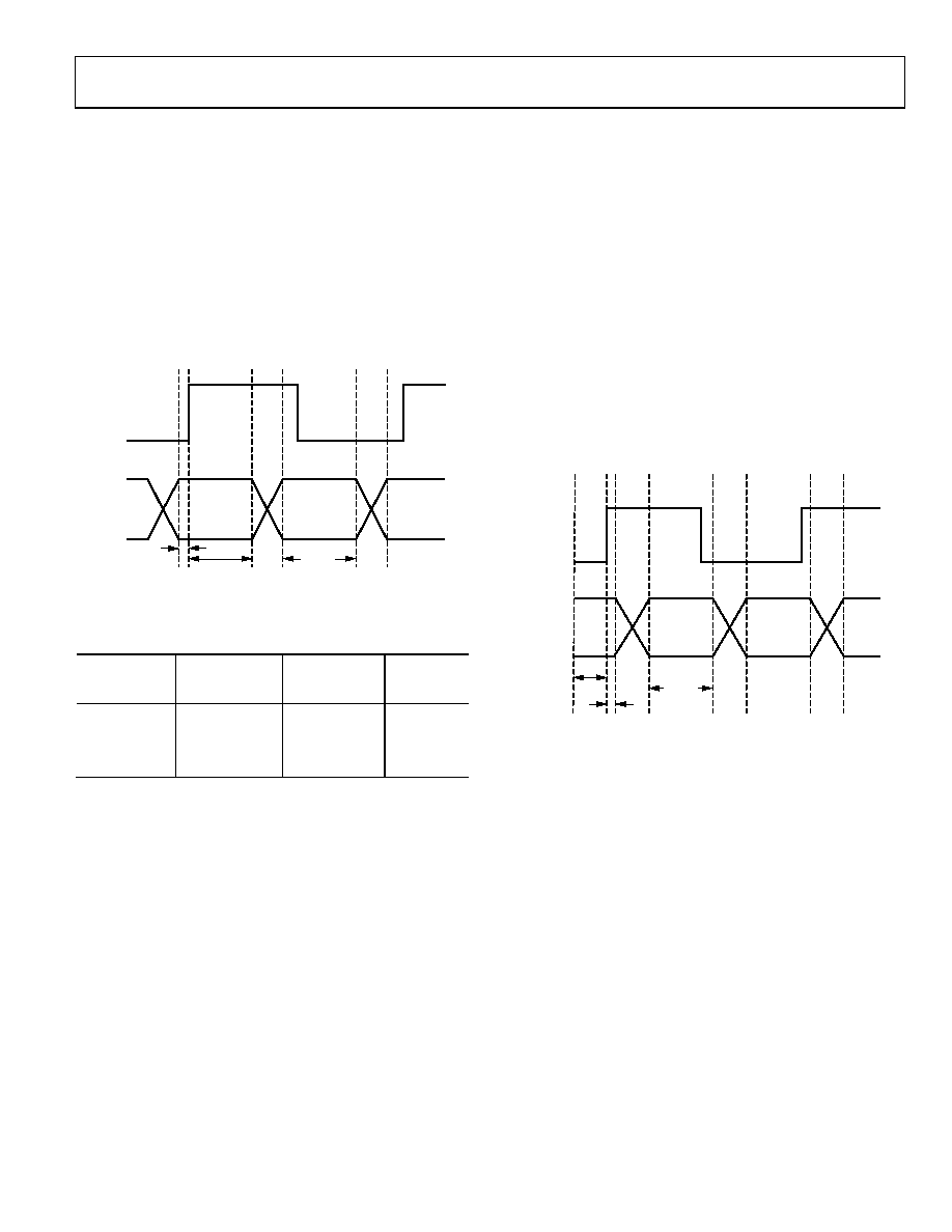
INTERFACE TIMING
The timing diagram for the digital interface port is shown in
Figure 37. When Register 0x16, Bits[2:0] are set to 000, the
sampling point of the data bus nominally occurs 165 ps after
each edge of the DCI signal and has an uncertainty of ±285 ps,
as illustrated by the data valid window shown in Figure 37. The
data and FRAME signals must be valid throughout this window.
The data and FRAME signals may change at any time between
data valid windows.
The setup (tS) and hold (tH) times, with respect to the edges,
are shown in Figure 37. The minimum setup and hold times
are shown in Table 14.
096
91
-042
DCI
DATA
tH
tS
DVW OR
KOW
NOTES
1. DVW = DATA VALID WINDOW. KOW = KEEP OUT WINDOW.
Figure 37. Timing Diagram for Input Data Port
Table 14. Data to DCI Setup and Hold Times
DCI Delay
Register 0x16,
Bits[1:0]
Minimum Setup
Time, tS (ns)
Minimum Hold
Time, tH (ns)
Sampling
Interval (ns)
00
0.12
0.45
0.57
01
0.01
0.74
0.73
10
0.2
1.03
0.83
11
0.28
1.16
0.88
Bypass DCI Delay Mode
An additional option for the timing of the data, DCI, and
FRAME signals requires the DCI to be delayed by 90° ahead
of the data and FRAME signals. In bypass DCI delay mode, the
DCI signal is placed in the optimal data valid window outside
the part, and the delay circuitry inside the part is bypassed. This
mode provides a smaller sampling window that allows for a wider
range of placement area for correct sampling edges. The bypass
DCI delay mode is enabled by setting Bit 2 in Register 0x16 to 1.
The sampling point of the data bus nominally occurs 90 ps before
each edge of the DCI signal and has an uncertainty of ±180 ps,
as illustrated by the sampling interval shown in Figure 38. The
resulting setup and hold times for this mode are as follows:
Minimum setup time (tS): 0.27 ns
Minimum hold time (tH): 0.09 ns
Sampling interval: 0.36 ns
Figure 38 shows the timing for the bypass DCI delay mode.
DCI
DATA
tH
tS
DVW OR
KOW
0
96
91-
099
NOTES
1. DVW = DATA VALID WINDOW. KOW = KEEP OUT WINDOW.
Figure 38. Timing Diagram for Input Data Port (Bypass DCI Delay Mode)
The data interface timing can be verified using the sample error
detection (SED) circuitry. See the Interface Timing Validation
section for more information.
相关PDF资料 |
PDF描述 |
|---|---|
| GTC02R-36-5P | CONN RCPT 4POS BOX MNT W/PINS |
| VE-2TY-MX-F2 | CONVERTER MOD DC/DC 3.3V 49.5W |
| MS27508E24B4PC | CONN RCPT 56POS BOX MNT W/PINS |
| VE-2TY-MW-F2 | CONVERTER MOD DC/DC 3.3V 66W |
| MS27508E24B4PB | CONN RCPT 56POS BOX MNT W/PINS |
相关代理商/技术参数 |
参数描述 |
|---|---|
| AD9146BCPZRL | 功能描述:IC DAC 16BIT SRL DUAL 48LFCSP RoHS:是 类别:集成电路 (IC) >> 数据采集 - 数模转换器 系列:TxDAC+® 产品培训模块:Lead (SnPb) Finish for COTS Obsolescence Mitigation Program 标准包装:1,000 系列:- 设置时间:1µs 位数:8 数据接口:串行 转换器数目:8 电压电源:双 ± 功率耗散(最大):941mW 工作温度:0°C ~ 70°C 安装类型:表面贴装 封装/外壳:24-SOIC(0.295",7.50mm 宽) 供应商设备封装:24-SOIC W 包装:带卷 (TR) 输出数目和类型:8 电压,单极 采样率(每秒):* |
| AD9146-EBZ | 制造商:Analog Devices 功能描述:16 BIT DUAL SIGNAL PROC DAC EB - Boxed Product (Development Kits) |
| AD9146-M5375-EBZ | 功能描述:BOARD EVAL FOR AD9146 DAC RoHS:是 类别:编程器,开发系统 >> 评估板 - 数模转换器 (DAC) 系列:TxDAC+® 产品培训模块:Lead (SnPb) Finish for COTS Obsolescence Mitigation Program 标准包装:1 系列:- DAC 的数量:4 位数:12 采样率(每秒):- 数据接口:串行,SPI? 设置时间:3µs DAC 型:电流/电压 工作温度:-40°C ~ 85°C 已供物品:板 已用 IC / 零件:MAX5581 |
| AD9148 | 制造商:AD 制造商全称:Analog Devices 功能描述:Quad 16-Bit,1 GSPS, TxDAC+ Digital-to-Analog Converter |
| AD9148ARUZ | 制造商:Analog Devices 功能描述:- Rail/Tube |
发布紧急采购,3分钟左右您将得到回复。