参数资料
| 型号: | AD9146BCPZRL |
| 厂商: | Analog Devices Inc |
| 文件页数: | 22/56页 |
| 文件大小: | 0K |
| 描述: | IC DAC 16BIT SRL DUAL 48LFCSP |
| 标准包装: | 2,500 |
| 系列: | TxDAC+® |
| 设置时间: | 20ns |
| 位数: | 16 |
| 数据接口: | 串行 |
| 转换器数目: | 2 |
| 电压电源: | 模拟和数字 |
| 工作温度: | -40°C ~ 85°C |
| 安装类型: | 表面贴装 |
| 封装/外壳: | 48-WFQFN 裸露焊盘,CSP |
| 供应商设备封装: | 48-LFCSP-WQ(7x7) |
| 包装: | 带卷 (TR) |
| 输出数目和类型: | 2 电流,单极 |
| 采样率(每秒): | 1.23G |
第1页第2页第3页第4页第5页第6页第7页第8页第9页第10页第11页第12页第13页第14页第15页第16页第17页第18页第19页第20页第21页当前第22页第23页第24页第25页第26页第27页第28页第29页第30页第31页第32页第33页第34页第35页第36页第37页第38页第39页第40页第41页第42页第43页第44页第45页第46页第47页第48页第49页第50页第51页第52页第53页第54页第55页第56页
Data Sheet
AD9146
Rev. A | Page 29 of 56
I AND Q
DACS
32
32 BITS
÷ INT
DCI
DACCLK
DATA
I AND Q
DATA
PATHS
DATA
FORMAT
INPUT
LATCH
REG 0
REG 1
REG 2
REG 3
REG 4
REG 5
REG 6
REG 7
RESET
LOGIC
FRAME
SYNC
FIFO SOFT ALIGN REQUEST
REG 0x18[1]
DATA/FIFO RATE
REG 0x10[6]
FIFO PHASE OFFSET
REG 0x17[2:0]
RE
AD
P
O
IN
T
E
R
RE
S
E
T
WR
IT
E
P
OIN
T
E
R
RE
S
E
T
READ
POINTER
WRITE
POINTER
09
69
1-
03
9
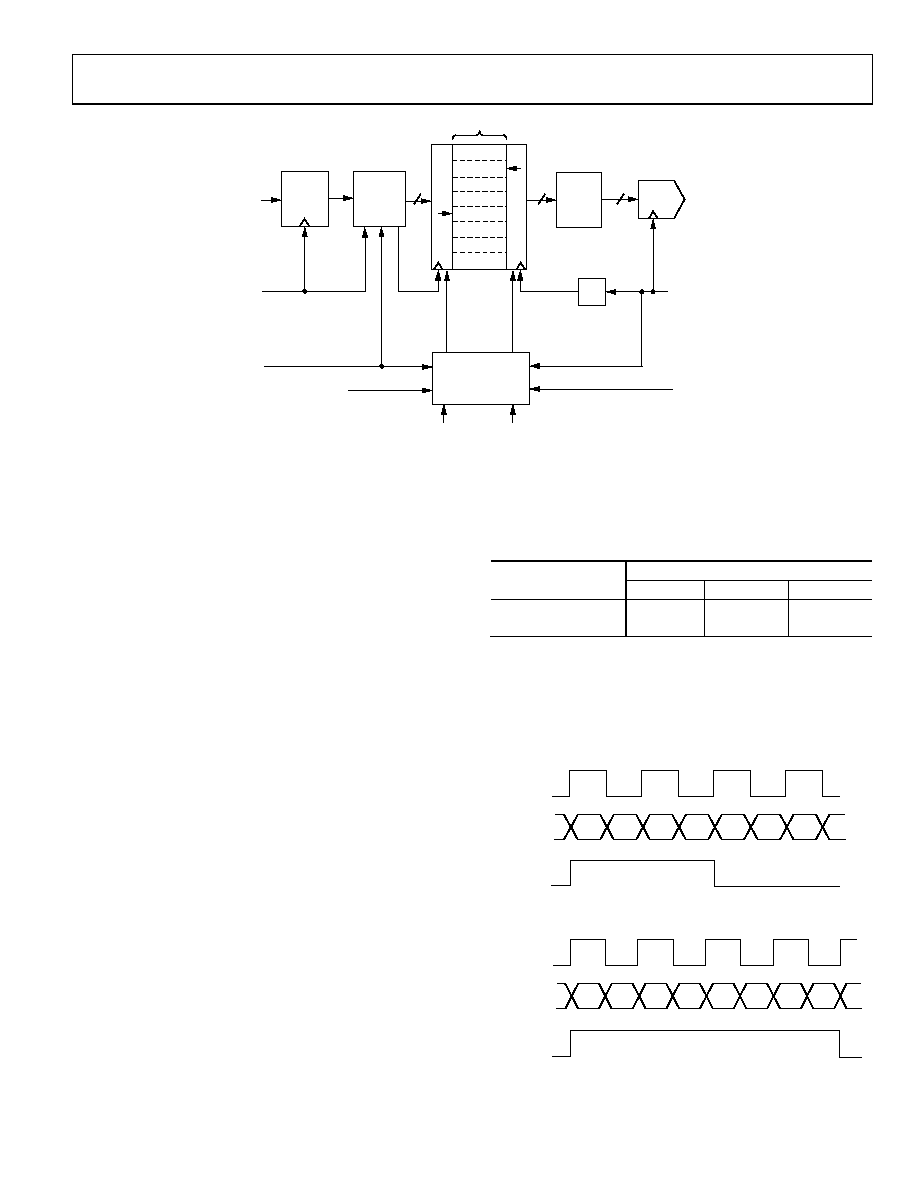
Figure 32. Block Diagram of FIFO
Nominally, data is written to and read from the FIFO at the same
rate. This keeps the FIFO depth constant. If data is written to the
FIFO faster than data is read out, the FIFO depth increases. If
data is read out of the FIFO faster than data is written to it, the
FIFO depth decreases. For optimum timing margin, the FIFO
depth should be maintained near half full (a difference of 4
between the write pointer and read pointer values). The FIFO
depth represents the FIFO pipeline delay and is part of the
overall latency of the AD9146.
Resetting the FIFO
When the AD9146 is powered on, the FIFO depth is unknown.
To avoid a concurrent read and write to the same FIFO address
and to ensure a fixed pipeline delay, it is important to reset the
FIFO pointers to known states. The FIFO pointers can be initial-
ized in two ways: via a write sequence to the serial port or by
strobing the FRAME input.
There are two types of FIFO reset: a relative reset and an absolute
reset. A relative reset enforces a defined FIFO depth. An absolute
reset enforces a particular write pointer value when the reset is
initiated. A serial port initiated FIFO reset is always a relative
reset. A FRAME strobe initiated reset can be either a relative or
an absolute reset.
The operation of the FRAME initiated FIFO reset depends on
the synchronization mode chosen.
When synchronization is disabled or when it is configured
for data rate mode synchronization, the FRAME strobe
initiates a relative FIFO reset. The reference point of the
relative reset is the position of the read pointer.
When FIFO mode synchronization is chosen, the FRAME
strobe initiates an absolute FIFO reset.
For more information about the synchronization function, see
the Multichip Synchronization section.
A summary of the synchronization modes and the types of
FIFO reset used is provided in Table 13.
Table 13. Summary of FIFO Resets
FIFO Reset Signal
Synchronization Mode
Disabled
Data Rate
FIFO Reset
Serial Port
Relative
FRAME
Relative
Absolute
For a FRAME dependent FIFO reset to occur, an extended
FRAME pulse must be sent to the part for proper operation.
The extended FRAME pulse must be asserted high for an entire
I and Q DAC data sample load. This corresponds to four data
clock samples in byte mode and eight data clock samples in
nibble mode (see Figure 33 and Figure 34, respectively).
Q0LSB
I1MSB
I1LSB
Q1MSB
Q1LSB
I2MSB
I2LSB
Q2MSB
Q2LSB
DCI
DATA
[15:0]
EXTENDED
FRAME
09
691
-09
7
Figure 33. Timing Diagram for Extended Frame Pulse (Byte Mode)
Q0N0
I1N3
I1N2
I1N1
I1N0
Q1N3
Q1N2
Q1N1
Q1N0
I2N3
DCI
DATA
[15:0]
EXTENDED
FRAME
0
9691-
098
Figure 34. Timing Diagram for Extended Frame Pulse (Nibble Mode)
相关PDF资料 |
PDF描述 |
|---|---|
| AD9267BCPZ | IC MOD SIGMA-DELTA DUAL 64LFCSP |
| AD9272BSVZRL-80 | IC ADC ASD OCTAL 80MSPS 100-TQFP |
| AD9273BBCZ-50 | IC ADCASD OCTAL 25MSPS 144CSPBGA |
| AD9276BSVZ | IC ADC 12BIT LNA/VGA/AAF 100TQFP |
| AD9277BSVZ | IC ADC 14BIT LNA/VGA/AAF 100TQFP |
相关代理商/技术参数 |
参数描述 |
|---|---|
| AD9146-EBZ | 制造商:Analog Devices 功能描述:16 BIT DUAL SIGNAL PROC DAC EB - Boxed Product (Development Kits) |
| AD9146-M5375-EBZ | 功能描述:BOARD EVAL FOR AD9146 DAC RoHS:是 类别:编程器,开发系统 >> 评估板 - 数模转换器 (DAC) 系列:TxDAC+® 产品培训模块:Lead (SnPb) Finish for COTS Obsolescence Mitigation Program 标准包装:1 系列:- DAC 的数量:4 位数:12 采样率(每秒):- 数据接口:串行,SPI? 设置时间:3µs DAC 型:电流/电压 工作温度:-40°C ~ 85°C 已供物品:板 已用 IC / 零件:MAX5581 |
| AD9148 | 制造商:AD 制造商全称:Analog Devices 功能描述:Quad 16-Bit,1 GSPS, TxDAC+ Digital-to-Analog Converter |
| AD9148ARUZ | 制造商:Analog Devices 功能描述:- Rail/Tube |
| AD9148BBCZ | 功能描述:IC DAC 16BIT QD 1GSPS 196CSPBGA RoHS:是 类别:集成电路 (IC) >> 数据采集 - 数模转换器 系列:TxDAC+® 标准包装:1 系列:- 设置时间:4.5µs 位数:12 数据接口:串行,SPI? 转换器数目:1 电压电源:单电源 功率耗散(最大):- 工作温度:-40°C ~ 125°C 安装类型:表面贴装 封装/外壳:8-SOIC(0.154",3.90mm 宽) 供应商设备封装:8-SOICN 包装:剪切带 (CT) 输出数目和类型:1 电压,单极;1 电压,双极 采样率(每秒):* 其它名称:MCP4921T-E/SNCTMCP4921T-E/SNRCTMCP4921T-E/SNRCT-ND |
发布紧急采购,3分钟左右您将得到回复。