参数资料
| 型号: | AD9146BCPZRL |
| 厂商: | Analog Devices Inc |
| 文件页数: | 38/56页 |
| 文件大小: | 0K |
| 描述: | IC DAC 16BIT SRL DUAL 48LFCSP |
| 标准包装: | 2,500 |
| 系列: | TxDAC+® |
| 设置时间: | 20ns |
| 位数: | 16 |
| 数据接口: | 串行 |
| 转换器数目: | 2 |
| 电压电源: | 模拟和数字 |
| 工作温度: | -40°C ~ 85°C |
| 安装类型: | 表面贴装 |
| 封装/外壳: | 48-WFQFN 裸露焊盘,CSP |
| 供应商设备封装: | 48-LFCSP-WQ(7x7) |
| 包装: | 带卷 (TR) |
| 输出数目和类型: | 2 电流,单极 |
| 采样率(每秒): | 1.23G |
第1页第2页第3页第4页第5页第6页第7页第8页第9页第10页第11页第12页第13页第14页第15页第16页第17页第18页第19页第20页第21页第22页第23页第24页第25页第26页第27页第28页第29页第30页第31页第32页第33页第34页第35页第36页第37页当前第38页第39页第40页第41页第42页第43页第44页第45页第46页第47页第48页第49页第50页第51页第52页第53页第54页第55页第56页
Data Sheet
AD9146
Rev. A | Page 43 of 56
DEVICE POWER MANAGEMENT
POWER DISSIPATION
The AD9146 has three supply rails: AVDD33, DVDD18, and
CVDD18.
The AVDD33 supply powers the DAC core circuitry. The power
dissipation of the AVDD33 supply rail is independent of the digital
operating mode and sample rate. The current drawn from the
AVDD33 supply rail is typically 54 mA (188 mW) when the full-
scale current of the I and Q DACs is set to the nominal value of
20 mA. Changing the full-scale current directly affects the supply
current drawn from the AVDD33 rail. For example, if the full-scale
current of the I DAC and the Q DAC is changed to 10 mA, the
AVDD33 supply current drops by 20 mA to 34 mA.
The DVDD18 supply powers all of the digital signal processing
blocks of the device. The serial port I/O pins, the RESET pin,
and the IRQ pin are also supplied from the DVDD18 power
supply. The power consumption from this supply is a function
of which digital blocks are enabled and the frequency at which
the device is operating.
The CVDD18 supply powers the clock receiver and clock distri-
bution circuitry. The power consumption from this supply varies
directly with the operating frequency of the device. CVDD18 also
powers the PLL. The power dissipation of the PLL is typically
80 mA when enabled.
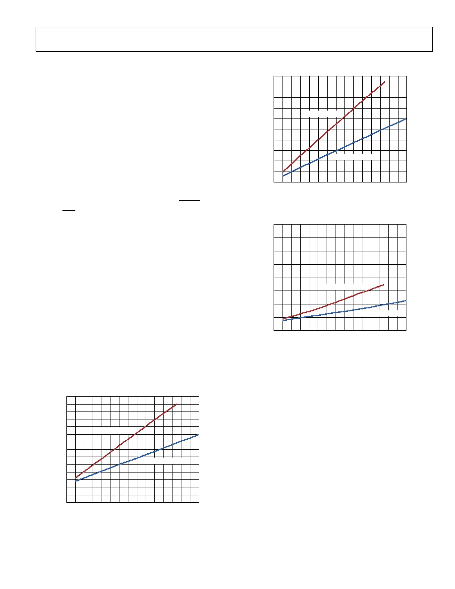
Figure 59 through Figure 61 show the power dissipation of
the AD9146 under a variety of operating conditions. All of the
graphs were taken with data being supplied to both the I and Q
DACs. The power consumption of the device does not vary
significantly with changes in the coarse modulation mode selected
or with the analog output frequency. Figure 59 shows the total
power dissipation. Figure 60 and Figure 61 show the power
dissipation of the DVDD18 and CVDD18 supplies.
Maximum power dissipation can be estimated to be 20% higher
than the typical power dissipation.
0
0.1
0.2
0.3
0.4
0.5
0.6
0.7
0.8
0.9
1.0
1.1
1.2
1.3
1.4
0
20 40 60 80 100 120 140 160 180 200 220 240 260 280 300
PO
W
ER
D
ISSI
PA
TION
(
W)
fDATA (MSPS)
09691-
100
4× INTERPOLATION
2× INTERPOLATION
Figure 59. Total Power Dissipation vs. fDATA Without PLL and Inverse Sinc
0
20 40 60 80 100 120 140 160 180 200 220 240 260 280 300
fDATA (MSPS)
0
0.1
0.2
0.3
0.4
0.5
0.6
0.7
0.8
0.9
1.0
PO
W
ER
D
ISSI
PA
TION
(
W)
09691-
101
4× INTERPOLATION
2× INTERPOLATION
Figure 60. DVDD18 Power Dissipation vs. fDATA Without Inverse Sinc
0
20 40 60 80 100 120 140 160 180 200 220 240 260 280 300
fDATA (MSPS)
0
0.05
0.10
0.15
0.20
0.25
0.30
0.35
0.40
PO
W
ER
D
ISSI
PA
TION
(
W)
09691-
102
4× INTERPOLATION
2× INTERPOLATION
Figure 61. CVDD18 Power Dissipation vs. fDATA with PLL Disabled
Tx ENABLE
The Tx enable feature provides additional power management
techniques that can be implemented in system applications. The
TXENABLE pin, when taken to a logic low, stops the trans-
mission of data from the part and clamps the outputs to midscale.
In addition, various portions of the DAC can be powered down
while the pin is held low, depending on the power saving require-
ments of the system and the amount of wake-up time required
when the pin is brought high.
Register 0x02 contains the bit controls to power down these
individual blocks: DAC cores, FIFO, interpolation filters, PLL,
and the internal reference. Depending on the power-down bits
selected, the necessary wake-up time and reprogramming of the
DAC may vary.
相关PDF资料 |
PDF描述 |
|---|---|
| AD9267BCPZ | IC MOD SIGMA-DELTA DUAL 64LFCSP |
| AD9272BSVZRL-80 | IC ADC ASD OCTAL 80MSPS 100-TQFP |
| AD9273BBCZ-50 | IC ADCASD OCTAL 25MSPS 144CSPBGA |
| AD9276BSVZ | IC ADC 12BIT LNA/VGA/AAF 100TQFP |
| AD9277BSVZ | IC ADC 14BIT LNA/VGA/AAF 100TQFP |
相关代理商/技术参数 |
参数描述 |
|---|---|
| AD9146-EBZ | 制造商:Analog Devices 功能描述:16 BIT DUAL SIGNAL PROC DAC EB - Boxed Product (Development Kits) |
| AD9146-M5375-EBZ | 功能描述:BOARD EVAL FOR AD9146 DAC RoHS:是 类别:编程器,开发系统 >> 评估板 - 数模转换器 (DAC) 系列:TxDAC+® 产品培训模块:Lead (SnPb) Finish for COTS Obsolescence Mitigation Program 标准包装:1 系列:- DAC 的数量:4 位数:12 采样率(每秒):- 数据接口:串行,SPI? 设置时间:3µs DAC 型:电流/电压 工作温度:-40°C ~ 85°C 已供物品:板 已用 IC / 零件:MAX5581 |
| AD9148 | 制造商:AD 制造商全称:Analog Devices 功能描述:Quad 16-Bit,1 GSPS, TxDAC+ Digital-to-Analog Converter |
| AD9148ARUZ | 制造商:Analog Devices 功能描述:- Rail/Tube |
| AD9148BBCZ | 功能描述:IC DAC 16BIT QD 1GSPS 196CSPBGA RoHS:是 类别:集成电路 (IC) >> 数据采集 - 数模转换器 系列:TxDAC+® 标准包装:1 系列:- 设置时间:4.5µs 位数:12 数据接口:串行,SPI? 转换器数目:1 电压电源:单电源 功率耗散(最大):- 工作温度:-40°C ~ 125°C 安装类型:表面贴装 封装/外壳:8-SOIC(0.154",3.90mm 宽) 供应商设备封装:8-SOICN 包装:剪切带 (CT) 输出数目和类型:1 电压,单极;1 电压,双极 采样率(每秒):* 其它名称:MCP4921T-E/SNCTMCP4921T-E/SNRCTMCP4921T-E/SNRCT-ND |
发布紧急采购,3分钟左右您将得到回复。