参数资料
| 型号: | AD9146BCPZRL |
| 厂商: | Analog Devices Inc |
| 文件页数: | 24/56页 |
| 文件大小: | 0K |
| 描述: | IC DAC 16BIT SRL DUAL 48LFCSP |
| 标准包装: | 2,500 |
| 系列: | TxDAC+® |
| 设置时间: | 20ns |
| 位数: | 16 |
| 数据接口: | 串行 |
| 转换器数目: | 2 |
| 电压电源: | 模拟和数字 |
| 工作温度: | -40°C ~ 85°C |
| 安装类型: | 表面贴装 |
| 封装/外壳: | 48-WFQFN 裸露焊盘,CSP |
| 供应商设备封装: | 48-LFCSP-WQ(7x7) |
| 包装: | 带卷 (TR) |
| 输出数目和类型: | 2 电流,单极 |
| 采样率(每秒): | 1.23G |
第1页第2页第3页第4页第5页第6页第7页第8页第9页第10页第11页第12页第13页第14页第15页第16页第17页第18页第19页第20页第21页第22页第23页当前第24页第25页第26页第27页第28页第29页第30页第31页第32页第33页第34页第35页第36页第37页第38页第39页第40页第41页第42页第43页第44页第45页第46页第47页第48页第49页第50页第51页第52页第53页第54页第55页第56页
AD9146
Data Sheet
Rev. A | Page 30 of 56
Serial Port Initiated FIFO Reset
A serial port initiated FIFO reset can be issued in any mode and
always results in a relative FIFO reset. To initialize the FIFO data
level through the serial port, Bit 1 of Register 0x18 should be
toggled from 0 to 1 and back. When the write to this register is
complete, the FIFO data level is initialized. When the initializa-
tion is triggered, the next time that the read pointer becomes 0,
the write pointer is set to the value of the FIFO start level variable
(Register 0x17, Bits[2:0]) upon initialization. By default, this
value is 4, but it can be programmed to a value from 0 to 7.
The recommended procedure for a serial port FIFO data level
initialization is as follows:
1.
Program Register 0x17 to 0x05.
2.
Request FIFO level reset by setting Register 0x18, Bit 1, to 1.
3.
Verify that the part acknowledges the request by ensuring
that Register 0x18, Bit 2, is set to 1.
4.
Remove the request by setting Register 0x18, Bit 1, to 0.
5.
Verify that the part drops the acknowledge signal by
ensuring that Register 0x18, Bit 2, is set to 0.
6.
Read back Register 0x19 to verify that the pointer spacing
is set to 3 (0x07) or 4 (0x0F).
7.
If the readback of Register 0x19 shows a pointer spacing
of 2 (0x03), increment Register 0x17 to a spacing of 0x06
and repeat Step 2 through Step 5. Read back Register 0x19
again to verify that the pointer spacing is now set to 3 (0x07).
8.
If the readback of Register 0x19 shows a pointer spacing
of 5 (0x1F) after Step 6, decrement Register 0x17 to a
spacing of 0x04 and repeat Step 2 through Step 5. Read
back Register 0x19 again to verify that the pointer spacing
is now set to 4 (0x0F).
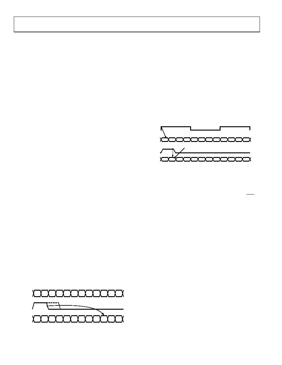
FRAME Initiated Relative FIFO Reset
The primary function of the FRAME input is to indicate to
which DAC the input data is written. Another function of the
FRAME input is to initialize the FIFO data level value. This is
done by asserting the FRAME signal high for at least the time
interval required to load complete data to the I and Q DACs.
This corresponds to four DCI periods in byte mode and eight
DCI periods in nibble mode.
To initiate a relative FIFO reset with the FRAME signal, the device
must be configured in data rate mode (Register 0x10, Bit 6 = 1).
When FRAME is asserted in data rate mode, the write pointer is
set to 4 by default (or to the FIFO start level) the next time that
the read pointer becomes 0 (see Figure 35).
09
69
1-
04
0
0
1
2
3
4
5
6
7
0
1
2
3
4
5
6
7
0
1
2
3
4
5
6
FIFO WRITE RESETS
READ
POINTER
FRAME
WRITE
POINTER
Figure 35. FRAME Input vs. Write Pointer Value, Data Rate Mode
FRAME Initiated Absolute FIFO Reset
In FIFO rate synchronization mode, the write pointer of the FIFO
is reset in an absolute manner. The synchronization signal aligns
the internal clocks on the part to a common reference clock so
that the pipeline delay in the digital circuit stays the same during
power cycles. The synchronization signal is sampled by the DAC
clock in the AD9146. The edge of the DAC clock used to sample
the synchronization signal is selected by Bit 3 of Register 0x10.
The FRAME signal is used to reset the FIFO write pointer. In
the FIFO rate synchronization mode, the FIFO write pointer is
reset immediately after the FRAME signal is asserted high for at
least the time interval required to load complete data to the I
and Q DACs. The FIFO write pointer is reset to the value of the
FIFO Phase Offset[2:0] bits in Register 0x17. FIFO rate synchro-
nization is selected by setting Bit 6 of Register 0x10 to 0.
READ
POINTER
WRITE
POINTER
SYNC
FRAME
FIFO READ RESET
FIFO WRITE
RESET
FIFO PHASE OFFSET[2:0]
REG 0x17[2:0] = 101
01
3
2
1
0
7
6
5
4
3
2
3
2
1
0
7
6
5
66
5
47
09
69
1
-04
1
Figure 36. FRAME Input vs. Write Pointer Value, FIFO Rate Mode
Monitoring the FIFO Status
The FIFO initialization and status can be read from Register 0x18.
This register provides information about the FIFO status and
whether the initialization was successful. The MSB of Register 0x18
is a FIFO warning flag that can optionally trigger a device IRQ.
This flag indicates that the FIFO is close to emptying (FIFO
level is 1) or overflowing (FIFO level is 7). In this case, data
may soon be corrupted, and action should be taken.
The FIFO data level can be read from Register 0x19 at any time.
The serial port reported FIFO data level is denoted as a 7-bit
thermometer code (Base 1 code) of the write counter state relative
to the absolute read counter being at 0. The optimum FIFO data
level of 4 is therefore reported as a value of 00001111 in the status
register.
Note that, depending on the timing relationship between the DCI
and the main DACCLK, the FIFO level value can be off by a ±1
count; that is, the readback of Register 0x19 can be 00011111 in
the case of a +1 count and 00000111 in the case of a 1 count.
Therefore, it is important to keep the difference between the
read and write pointers to a value of at least 2.
相关PDF资料 |
PDF描述 |
|---|---|
| AD9267BCPZ | IC MOD SIGMA-DELTA DUAL 64LFCSP |
| AD9272BSVZRL-80 | IC ADC ASD OCTAL 80MSPS 100-TQFP |
| AD9273BBCZ-50 | IC ADCASD OCTAL 25MSPS 144CSPBGA |
| AD9276BSVZ | IC ADC 12BIT LNA/VGA/AAF 100TQFP |
| AD9277BSVZ | IC ADC 14BIT LNA/VGA/AAF 100TQFP |
相关代理商/技术参数 |
参数描述 |
|---|---|
| AD9146-EBZ | 制造商:Analog Devices 功能描述:16 BIT DUAL SIGNAL PROC DAC EB - Boxed Product (Development Kits) |
| AD9146-M5375-EBZ | 功能描述:BOARD EVAL FOR AD9146 DAC RoHS:是 类别:编程器,开发系统 >> 评估板 - 数模转换器 (DAC) 系列:TxDAC+® 产品培训模块:Lead (SnPb) Finish for COTS Obsolescence Mitigation Program 标准包装:1 系列:- DAC 的数量:4 位数:12 采样率(每秒):- 数据接口:串行,SPI? 设置时间:3µs DAC 型:电流/电压 工作温度:-40°C ~ 85°C 已供物品:板 已用 IC / 零件:MAX5581 |
| AD9148 | 制造商:AD 制造商全称:Analog Devices 功能描述:Quad 16-Bit,1 GSPS, TxDAC+ Digital-to-Analog Converter |
| AD9148ARUZ | 制造商:Analog Devices 功能描述:- Rail/Tube |
| AD9148BBCZ | 功能描述:IC DAC 16BIT QD 1GSPS 196CSPBGA RoHS:是 类别:集成电路 (IC) >> 数据采集 - 数模转换器 系列:TxDAC+® 标准包装:1 系列:- 设置时间:4.5µs 位数:12 数据接口:串行,SPI? 转换器数目:1 电压电源:单电源 功率耗散(最大):- 工作温度:-40°C ~ 125°C 安装类型:表面贴装 封装/外壳:8-SOIC(0.154",3.90mm 宽) 供应商设备封装:8-SOICN 包装:剪切带 (CT) 输出数目和类型:1 电压,单极;1 电压,双极 采样率(每秒):* 其它名称:MCP4921T-E/SNCTMCP4921T-E/SNRCTMCP4921T-E/SNRCT-ND |
发布紧急采购,3分钟左右您将得到回复。