- 您现在的位置:买卖IC网 > PDF目录16854 > AD9517-3A/PCBZ (Analog Devices Inc)BOARD EVALUATION FOR AD9517-3A PDF资料下载
参数资料
| 型号: | AD9517-3A/PCBZ |
| 厂商: | Analog Devices Inc |
| 文件页数: | 39/80页 |
| 文件大小: | 0K |
| 描述: | BOARD EVALUATION FOR AD9517-3A |
| 设计资源: | AD9517 Eval Brd Schematics AD9517 Gerber Files AD9517-3 BOM |
| 标准包装: | 1 |
| 主要目的: | 计时,时钟发生器 |
| 嵌入式: | 否 |
| 已用 IC / 零件: | AD9517-3A |
| 主要属性: | 2 输入,12 输出,2.0GHz VCO |
| 次要属性: | CMOS,LVPECL 和 LVDS 兼容 |
| 已供物品: | 板 |
第1页第2页第3页第4页第5页第6页第7页第8页第9页第10页第11页第12页第13页第14页第15页第16页第17页第18页第19页第20页第21页第22页第23页第24页第25页第26页第27页第28页第29页第30页第31页第32页第33页第34页第35页第36页第37页第38页当前第39页第40页第41页第42页第43页第44页第45页第46页第47页第48页第49页第50页第51页第52页第53页第54页第55页第56页第57页第58页第59页第60页第61页第62页第63页第64页第65页第66页第67页第68页第69页第70页第71页第72页第73页第74页第75页第76页第77页第78页第79页第80页
AD9517-3
Data Sheet
Rev. E | Page 44 of 80
Phase Offset or Coarse Time Delay (0, 1)
Each channel divider allows for a phase offset, or a coarse time
delay, to be programmed by setting register bits (see Table 38).
These settings determine the number of cycles (successive
rising edges) of the channel divider input frequency by which to
offset, or delay, the rising edge of the output of the divider. This
delay is with respect to a nondelayed output (that is, with a
phase offset of zero). The amount of the delay is set by five bits
loaded into the phase offset (PO) register plus the start high (SH)
bit for each channel divider. When the start high bit is set, the
delay is also affected by the number of low cycles (M) that are
programmed for the divider.
The sync function must be used to make phase offsets effective
(see the Synchronizing the Outputs—Sync Function section).
Table 38. Setting Phase Offset and Division for Divider 0 and
Divider 1
Divider
Start
High (SH)
Phase
Offset (PO)
Low Cycles
M
High Cycles
N
0
0x191[4]
0x191[3:0]
0x190[7:4]
0x190[3:0]
1
0x197[4]
0x197[3:0]
0x196[7:4]
0x196[3:0]
Let
Δt = delay (in seconds).
Δc = delay (in cycles of clock signal at input to DX).
TX = period of the clock signal at the input of the divider, DX
(in seconds).
Φ = 16 × SH[4] + 8 × PO[3] + 4 × PO[2] + 2 × PO[1] + 1 × PO[0]
The channel divide-by is set as N = high cycles and M = low cycles.
Case 1
For Φ ≤ 15:
Δt = Φ × TX
Δc = Δt/TX = Φ
Case 2
For Φ ≥ 16:
Δt = (Φ 16 + M + 1) × TX
Δc = Δt/TX
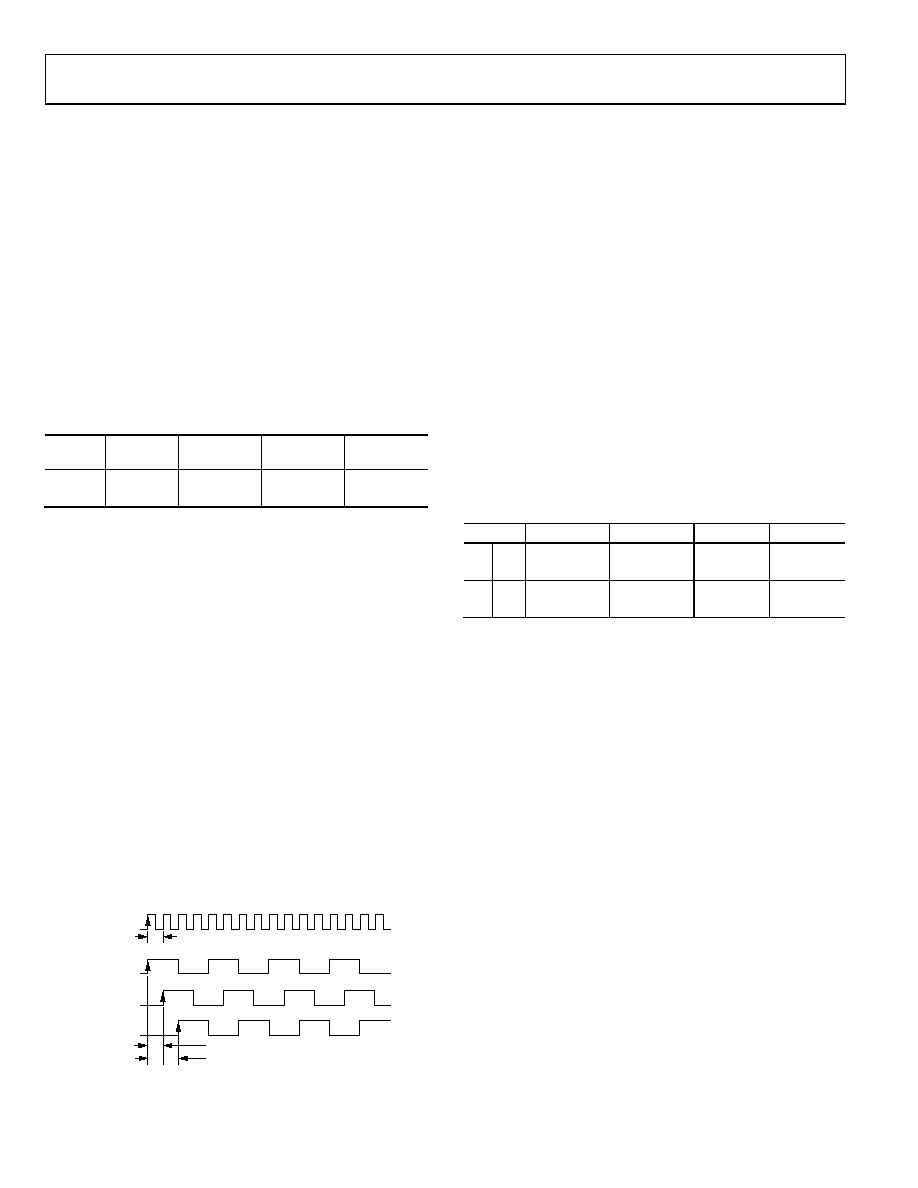
By giving each divider a different phase offset, output-to-output
delays can be set in increments of the channel divider input
clock cycle. Figure 55 shows the results of setting such a coarse
offset between outputs.
CHANNEL DIVIDER OUTPUTS
DIV = 4, DUTY = 50%
01
23
456
78
9 10 11 12 13 14 15
Tx
DIVIDER 0
DIVIDER 1
DIVIDER 2
CHANNEL
DIVIDER INPUT
SH = 0
PO = 0
SH = 0
PO = 1
SH = 0
PO = 2
1 × Tx
2 × Tx
0
6427-
071
Figure 55. Effect of Coarse Phase Offset (or Delay)
Channel Dividers—LVDS/CMOS Outputs
Channel Divider 2 and Channel Divider 3 each drive a pair of
LVDS outputs, giving a total of four LVDS outputs (OUT4 to
OUT7). Alternatively, each of these LVDS differential outputs
can be configured individually as a pair (A and B) of CMOS
single-ended outputs, providing for up to eight CMOS outputs.
By default, the B output of each pair is off but can be turned on
as desired.
Channel Divider 2 and Channel Divider 3 each consist of two
cascaded, 2 to 32, frequency dividers. The channel frequency
division is DX.1 × DX.2 or up to 1024. Divide-by-1 is achieved by
bypassing one or both of these dividers. Both of the dividers
also have DCC enabled by default, but this function can be
disabled, if desired, by setting the DCCOFF bit of the channel.
A coarse phase offset or delay is also programmable (see the
section). The channel dividers operate up to 1600 MHz. The
features and settings of the dividers are selected by programming
the appropriate setup and control registers (see Table 52 and
Divider
M
N
Bypass
DCCOFF
2
2.1
0x199[7:4]
0x199[3:0]
0x19C[4]
0x19D[0]
2.2
0x19B[7:4]
0x19B[3:0]
0x19C[5]
0x19D[0]
3
3.1
0x19E[7:4]
0x19E[3:0]
0x1A1[4]
0x1A2[0]
3.2
0x1A0[7:4]
0x1A0[3:0]
0x1A1[5]
0x1A2[0]
1 Note that the value stored in the register = # of cycles minus 1.
Channel Frequency Division (Divider 2 and Divider 3)
The division for each channel divider is set by the bits in the
registers for the individual dividers (X.Y = 2.1, 2.2, 3.1, and 3.2)
Number of Low Cycles = MX.Y + 1
Number of High Cycles = NX.Y + 1
When both X.1 and X.2 are bypassed, DX = 1 × 1 = 1.
When only X.2 is bypassed, DX = (NX.1 + MX.1 + 2) × 1.
When both X.1 and X.2 are not bypassed, DX = (NX.1 + MX.1 + 2) ×
(NX.2 + MX.2 + 2).
By cascading the dividers, channel division up to 1024 can be
obtained. However, not all integer value divisions from 1 to
1024 are obtainable; only the values that are the product of the
separate divisions of the two dividers (DX.1 × DX.2) can be realized.
If only one divider is needed when using Divider 2 and Divider 3,
use the first one (X.1) and bypass the second one (X.2). Do not
bypass X.1 and use X.2.
相关PDF资料 |
PDF描述 |
|---|---|
| ADM1191-2ARMZ-R7 | IC PWR MONITOR DGTL ALERT 10MSOP |
| ADCLK954/PCBZ | KIT EVAL CLK BUFF ADCLK954 |
| RNF-100-MINI-SPL-3/32-BK | HEATSHRINK RNF-100 3/32"X65'BLK |
| AD9522-0/PCBZ | BOARD EVAL FOR AD9522-0 CLK GEN |
| EBM22DCMT-S288 | CONN EDGECARD 44POS .156 EXTEND |
相关代理商/技术参数 |
参数描述 |
|---|---|
| AD9517-3BCPZ | 制造商:Analog Devices 功能描述: |
| AD9517-3BCPZ-REEL7 | 制造商:Analog Devices 功能描述: |
| AD9517-3BCPZ-TR | 制造商:Analog Devices 功能描述:12-OUTPUT CLOCK GENERATOR WITH INTEGRATED 2.0 GHZ VCO - Tape and Reel |
| AD9517-4 | 制造商:AD 制造商全称:Analog Devices 功能描述:12-Output Clock Generator with Integrated 1.6 GHz VCO |
| AD9517-4A/PCBZ | 功能描述:BOARD EVALUATION FOR AD9517-4A RoHS:是 类别:编程器,开发系统 >> 评估演示板和套件 系列:- 标准包装:1 系列:- 主要目的:电信,线路接口单元(LIU) 嵌入式:- 已用 IC / 零件:IDT82V2081 主要属性:T1/J1/E1 LIU 次要属性:- 已供物品:板,电源,线缆,CD 其它名称:82EBV2081 |
发布紧急采购,3分钟左右您将得到回复。