- 您现在的位置:买卖IC网 > PDF目录16854 > AD9517-3A/PCBZ (Analog Devices Inc)BOARD EVALUATION FOR AD9517-3A PDF资料下载
参数资料
| 型号: | AD9517-3A/PCBZ |
| 厂商: | Analog Devices Inc |
| 文件页数: | 70/80页 |
| 文件大小: | 0K |
| 描述: | BOARD EVALUATION FOR AD9517-3A |
| 设计资源: | AD9517 Eval Brd Schematics AD9517 Gerber Files AD9517-3 BOM |
| 标准包装: | 1 |
| 主要目的: | 计时,时钟发生器 |
| 嵌入式: | 否 |
| 已用 IC / 零件: | AD9517-3A |
| 主要属性: | 2 输入,12 输出,2.0GHz VCO |
| 次要属性: | CMOS,LVPECL 和 LVDS 兼容 |
| 已供物品: | 板 |
第1页第2页第3页第4页第5页第6页第7页第8页第9页第10页第11页第12页第13页第14页第15页第16页第17页第18页第19页第20页第21页第22页第23页第24页第25页第26页第27页第28页第29页第30页第31页第32页第33页第34页第35页第36页第37页第38页第39页第40页第41页第42页第43页第44页第45页第46页第47页第48页第49页第50页第51页第52页第53页第54页第55页第56页第57页第58页第59页第60页第61页第62页第63页第64页第65页第66页第67页第68页第69页当前第70页第71页第72页第73页第74页第75页第76页第77页第78页第79页第80页
AD9517-3
Data Sheet
Rev. E | Page 72 of 80
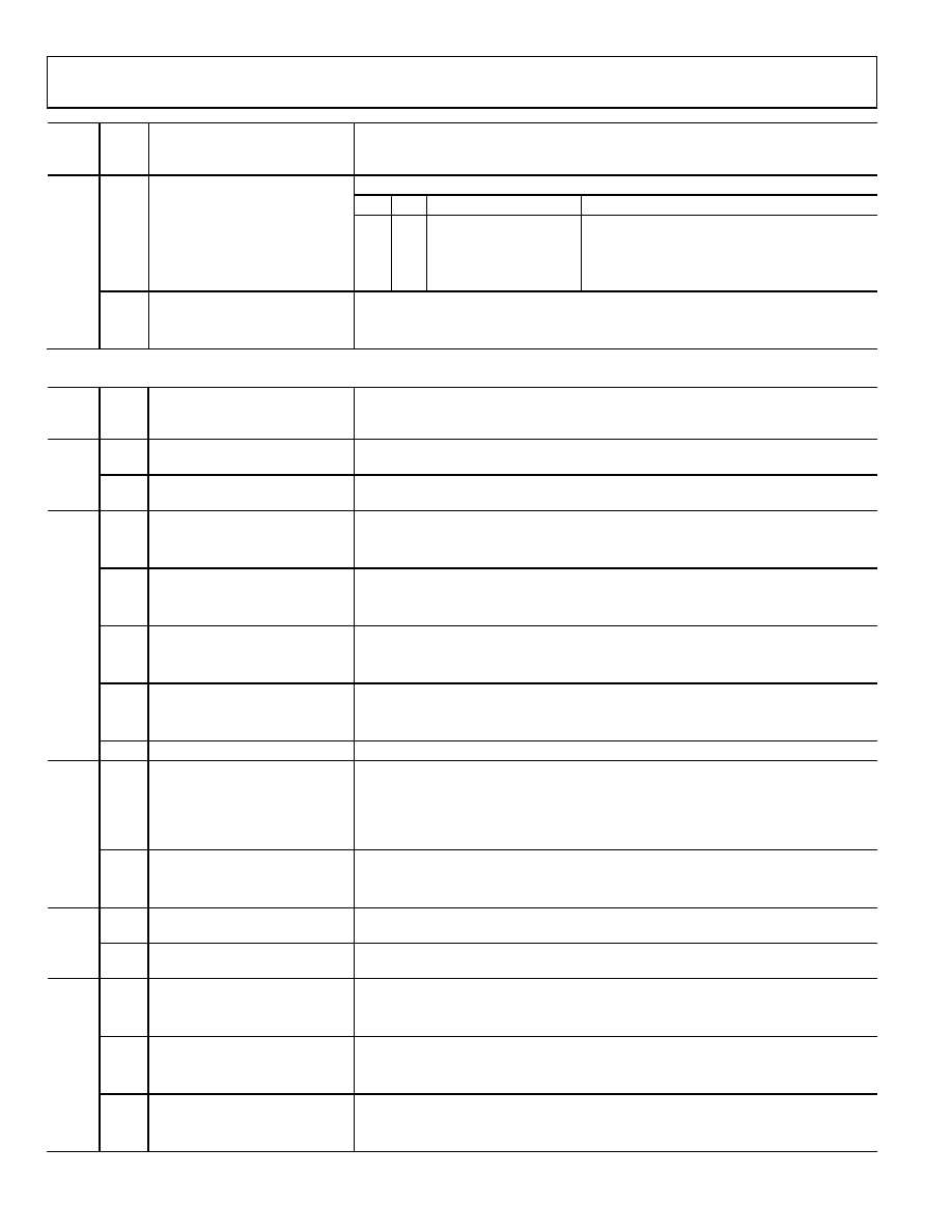
Reg.
Addr.
(Hex)
Bits
Name
Description
0x143
[2:1]
OUT7 LVDS output current
Sets output current level in LVDS mode. This has no effect in CMOS mode.
2
1
Current (mA)
Recommended Termination ()
0
1.75
100
0
1
3.5
100 (default)
1
0
5.25
50
1
7
50
0
OUT7 power-down
Powers down output (LVDS/CMOS).
0: power on.
1: power off (default).
Table 58. LVPECL Channel Dividers
Reg.
Addr.
(Hex)
Bits
Name
Description
0x190
[7:4]
Divider 0 low cycles
Number of clock cycles (minus 1) of the divider input during which divider output stays
low. A value of 0x0 means that the divider is low for one input clock cycle (default = 0x0).
[3:0]
Divider 0 high cycles
Number of clock cycles (minus 1) of the divider input during which divider output stays
high. A value of 0x0 means that the divider is high for one input clock cycle (default = 0x0).
0x191
7
Divider 0 bypass
Bypasses and powers down the divider; routes input to divider output.
0: uses divider.
1: bypasses divider (default).
6
Divider 0 nosync
No sync.
0: obeys chip-level SYNC signal (default).
1: ignores chip-level SYNC signal.
5
Divider 0 force high
Forces divider output to high. This requires that nosync (Bit 6) also be set.
0: divider output forced to low (default).
1: divider output forced to high.
4
Divider 0 start high
Selects clock output to start high or start low.
0: starts low (default).
1: starts high.
[3:0]
Divider 0 phase offset
Phase offset (default = 0x0).
0x192
1
Divider 0 direct to output
Connects OUT0 and OUT1 to Divider 0 or directly to VCO or CLK.
0: OUT0 and OUT1 are connected to Divider 0 (default).
1: If Register 0x1E1[1:0] = 10b, the VCO is routed directly to OUT0 and OUT1.
If Register 0x1E1[1:0] = 00b, the CLK is routed directly to OUT0 and OUT1.
If Register 0x1E1[1:0] = 01b, there is no effect.
0
Divider 0 DCCOFF
Duty-cycle correction function.
0: enables duty-cycle correction (default).
1: disables duty-cycle correction.
0x196
[7:4]
Divider 1 low cycles
Number of clock cycles of the divider input during which divider output stays low.
A value of 0x0 means that the divider is low for one input clock cycle (default = 0x0).
[3:0]
Divider 1 high cycles
Number of clock cycles (minus 1) of the divider input during which divider output stays
high. A value of 0x0 means that the divider is high for one input clock cycle (default = 0x0).
0x197
7
Divider 1 bypass
Bypasses and powers down the divider; routes input to divider output.
0: uses divider (default).
1: bypasses divider.
6
Divider 1 nosync
No sync.
0: obeys chip-level SYNC signal (default).
1: ignores chip-level SYNC signal.
5
Divider 1 force high
Forces divider output to high. This requires that nosync (Bit 6) also be set.
0: divider output forced to low (default).
1: divider output forced to high.
相关PDF资料 |
PDF描述 |
|---|---|
| ADM1191-2ARMZ-R7 | IC PWR MONITOR DGTL ALERT 10MSOP |
| ADCLK954/PCBZ | KIT EVAL CLK BUFF ADCLK954 |
| RNF-100-MINI-SPL-3/32-BK | HEATSHRINK RNF-100 3/32"X65'BLK |
| AD9522-0/PCBZ | BOARD EVAL FOR AD9522-0 CLK GEN |
| EBM22DCMT-S288 | CONN EDGECARD 44POS .156 EXTEND |
相关代理商/技术参数 |
参数描述 |
|---|---|
| AD9517-3BCPZ | 制造商:Analog Devices 功能描述: |
| AD9517-3BCPZ-REEL7 | 制造商:Analog Devices 功能描述: |
| AD9517-3BCPZ-TR | 制造商:Analog Devices 功能描述:12-OUTPUT CLOCK GENERATOR WITH INTEGRATED 2.0 GHZ VCO - Tape and Reel |
| AD9517-4 | 制造商:AD 制造商全称:Analog Devices 功能描述:12-Output Clock Generator with Integrated 1.6 GHz VCO |
| AD9517-4A/PCBZ | 功能描述:BOARD EVALUATION FOR AD9517-4A RoHS:是 类别:编程器,开发系统 >> 评估演示板和套件 系列:- 标准包装:1 系列:- 主要目的:电信,线路接口单元(LIU) 嵌入式:- 已用 IC / 零件:IDT82V2081 主要属性:T1/J1/E1 LIU 次要属性:- 已供物品:板,电源,线缆,CD 其它名称:82EBV2081 |
发布紧急采购,3分钟左右您将得到回复。