- 您现在的位置:买卖IC网 > PDF目录16854 > AD9517-3A/PCBZ (Analog Devices Inc)BOARD EVALUATION FOR AD9517-3A PDF资料下载
参数资料
| 型号: | AD9517-3A/PCBZ |
| 厂商: | Analog Devices Inc |
| 文件页数: | 45/80页 |
| 文件大小: | 0K |
| 描述: | BOARD EVALUATION FOR AD9517-3A |
| 设计资源: | AD9517 Eval Brd Schematics AD9517 Gerber Files AD9517-3 BOM |
| 标准包装: | 1 |
| 主要目的: | 计时,时钟发生器 |
| 嵌入式: | 否 |
| 已用 IC / 零件: | AD9517-3A |
| 主要属性: | 2 输入,12 输出,2.0GHz VCO |
| 次要属性: | CMOS,LVPECL 和 LVDS 兼容 |
| 已供物品: | 板 |
第1页第2页第3页第4页第5页第6页第7页第8页第9页第10页第11页第12页第13页第14页第15页第16页第17页第18页第19页第20页第21页第22页第23页第24页第25页第26页第27页第28页第29页第30页第31页第32页第33页第34页第35页第36页第37页第38页第39页第40页第41页第42页第43页第44页当前第45页第46页第47页第48页第49页第50页第51页第52页第53页第54页第55页第56页第57页第58页第59页第60页第61页第62页第63页第64页第65页第66页第67页第68页第69页第70页第71页第72页第73页第74页第75页第76页第77页第78页第79页第80页
Data Sheet
AD9517-3
Rev. E | Page 5 of 80
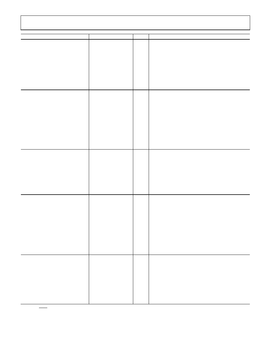
Parameter
Min
Typ
Max
Unit
Test Conditions/Comments
CHARGE PUMP (CP)
CPV is CP pin voltage; VCP is charge pump power supply voltage
ICP Sink/Source
Programmable
High Value
4.8
mA
With CPRSET = 5.1 k
Low Value
0.60
mA
Absolute Accuracy
2.5
%
CPV = VCP/2 V
CPRSET Range
2.7/10
k
ICP High Impedance Mode Leakage
1
nA
Sink-and-Source Current Matching
2
%
0.5 < CPV < VCP 0.5 V
ICP vs. CPV
1.5
%
0.5 < CPV < VCP 0.5 V
ICP vs. Temperature
2
%
CPV = VCP/2 V
PRESCALER (PART OF N DIVIDER)
See the
Prescaler Input Frequency
P = 1 FD
300
MHz
P = 2 FD
600
MHz
P = 3 FD
900
MHz
P = 2 DM (2/3)
200
MHz
P = 4 DM (4/5)
1000
MHz
P = 8 DM (8/9)
2400
MHz
P = 16 DM (16/17)
3000
MHz
P = 32 DM (32/33)
3000
MHz
Prescaler Output Frequency
300
MHz
A, B counter input frequency (prescaler input frequency
divided by P)
PLL DIVIDER DELAYS
Register 0x019: R, Bits[5:3]; N, Bits[2:0]; see Table 54
000
Off
ps
001
330
ps
010
440
ps
011
550
ps
100
660
ps
101
770
ps
110
880
ps
111
990
ps
NOISE CHARACTERISTICS
In-Band Phase Noise of the Charge
Pump/Phase Frequency Detector
(In-Band Is Within the LBW of the PLL)
The PLL in-band phase noise floor is estimated by measuring
the in-band phase noise at the output of the VCO and
subtracting 20 log(N) (where N is the value of the N divider)
At 500 kHz PFD Frequency
165
dBc/Hz
At 1 MHz PFD Frequency
162
dBc/Hz
At 10 MHz PFD Frequency
151
dBc/Hz
At 50 MHz PFD Frequency
143
dBc/Hz
PLL Figure of Merit (FOM)
220
dBc/Hz
Reference slew rate > 0.25 V/ns; FOM +10 log(fPFD) is an approxi-
mation of the PFD/CP in-band phase noise (in the flat region)
inside the PLL loop bandwidth; when running closed-loop, the
phase noise, as observed at the VCO output, is increased by
20 log(N)
PLL DIGITAL LOCK DETECT WINDOW2
Signal available at LD, STATUS, and REFMON pins
when selected by appropriate register settings
Required to Lock (Coincidence of Edges)
Selected by Register 0x017[1:0] and Register 0x018[4]
Low Range (ABP 1.3 ns, 2.9 ns)
3.5
ns
Register 0x017[1:0] = 00b, 01b, 11b; Register 0x018[4] = 1b
High Range (ABP 1.3 ns, 2.9 ns)
7.5
ns
Register 0x017[1:0] = 00b, 01b, 11b; Register 0x018[4] = 0b
High Range (ABP 6.0 ns)
3.5
ns
Register 0x017[1:0] = 10b; Register 0x018[4] = 0b
To Unlock After Lock (Hysteresis)2
Low Range (ABP 1.3 ns, 2.9 ns)
7
ns
Register 0x017[1:0] = 00b, 01b, 11b; Register 0x018[4] = 1b
High Range (ABP 1.3 ns, 2.9 ns)
15
ns
Register 0x017[1:0] = 00b, 01b, 11b; Register 0x018[4] = 0b
High Range (ABP 6.0 ns)
11
ns
Register 0x017[1:0] = 10b; Register 0x018[4] = 0b
1
REFIN and REFIN self-bias points are offset slightly to avoid chatter on an open input condition.
2
For reliable operation of the digital lock detect, the period of the PFD frequency must be greater than the unlock-after-lock time.
相关PDF资料 |
PDF描述 |
|---|---|
| ADM1191-2ARMZ-R7 | IC PWR MONITOR DGTL ALERT 10MSOP |
| ADCLK954/PCBZ | KIT EVAL CLK BUFF ADCLK954 |
| RNF-100-MINI-SPL-3/32-BK | HEATSHRINK RNF-100 3/32"X65'BLK |
| AD9522-0/PCBZ | BOARD EVAL FOR AD9522-0 CLK GEN |
| EBM22DCMT-S288 | CONN EDGECARD 44POS .156 EXTEND |
相关代理商/技术参数 |
参数描述 |
|---|---|
| AD9517-3BCPZ | 制造商:Analog Devices 功能描述: |
| AD9517-3BCPZ-REEL7 | 制造商:Analog Devices 功能描述: |
| AD9517-3BCPZ-TR | 制造商:Analog Devices 功能描述:12-OUTPUT CLOCK GENERATOR WITH INTEGRATED 2.0 GHZ VCO - Tape and Reel |
| AD9517-4 | 制造商:AD 制造商全称:Analog Devices 功能描述:12-Output Clock Generator with Integrated 1.6 GHz VCO |
| AD9517-4A/PCBZ | 功能描述:BOARD EVALUATION FOR AD9517-4A RoHS:是 类别:编程器,开发系统 >> 评估演示板和套件 系列:- 标准包装:1 系列:- 主要目的:电信,线路接口单元(LIU) 嵌入式:- 已用 IC / 零件:IDT82V2081 主要属性:T1/J1/E1 LIU 次要属性:- 已供物品:板,电源,线缆,CD 其它名称:82EBV2081 |
发布紧急采购,3分钟左右您将得到回复。