- 您现在的位置:买卖IC网 > PDF目录9085 > AD9520-1BCPZ-REEL7 (Analog Devices Inc)IC CLOCK GEN 2.5GHZ VCO 64LFCSP PDF资料下载
参数资料
| 型号: | AD9520-1BCPZ-REEL7 |
| 厂商: | Analog Devices Inc |
| 文件页数: | 26/80页 |
| 文件大小: | 0K |
| 描述: | IC CLOCK GEN 2.5GHZ VCO 64LFCSP |
| 设计资源: | Synchronizing Multiple AD9910 1 GSPS Direct Digital Synthesizers (CN0121) Phase Coherent FSK Modulator (CN0186) |
| 标准包装: | 750 |
| 类型: | 时钟发生器,扇出配送 |
| PLL: | 是 |
| 输入: | CMOS,LVDS,LVPECL |
| 输出: | CMOS,LVPECL |
| 电路数: | 1 |
| 比率 - 输入:输出: | 2:12,2:24 |
| 差分 - 输入:输出: | 是/是 |
| 频率 - 最大: | 2.65GHz |
| 除法器/乘法器: | 是/无 |
| 电源电压: | 3.135 V ~ 3.465 V |
| 工作温度: | -40°C ~ 85°C |
| 安装类型: | 表面贴装 |
| 封装/外壳: | 64-VFQFN 裸露焊盘,CSP |
| 供应商设备封装: | 64-LFCSP-VQ(9x9) |
| 包装: | 带卷 (TR) |
| 配用: | AD9520-1/PCBZ-ND - BOARD EVAL FOR AD9520-1 |
第1页第2页第3页第4页第5页第6页第7页第8页第9页第10页第11页第12页第13页第14页第15页第16页第17页第18页第19页第20页第21页第22页第23页第24页第25页当前第26页第27页第28页第29页第30页第31页第32页第33页第34页第35页第36页第37页第38页第39页第40页第41页第42页第43页第44页第45页第46页第47页第48页第49页第50页第51页第52页第53页第54页第55页第56页第57页第58页第59页第60页第61页第62页第63页第64页第65页第66页第67页第68页第69页第70页第71页第72页第73页第74页第75页第76页第77页第78页第79页第80页
AD9520-1
Data Sheet
Rev. A | Page 32 of 80
Mode 2—High Frequency Clock Distribution; CLK or
External VCO > 1600 MHz
The AD9520 power-up default configuration has the PLL
powered off and the routing of the input set so that the CLK/
CLK input is connected to the distribution section through the
VCO divider (divide-by-1/divide-by-2/divide-by-3/divide-by-4/
divide-by-5/divide-by-6). This is a distribution only mode that
allows for an external input up to 2400 MHz (see Table 3). The
maximum frequency that can be applied to the channel dividers
is 1600 MHz; therefore, higher input frequencies must be divided
down before reaching the channel dividers.
When the PLL is enabled, this routing also allows the use of the
PLL with an external VCO or VCXO with a frequency of less than
2400 MHz. In this configuration, the internal VCO is not used and
is powered off. The external VCO/VCXO feeds directly into the
prescaler.
The register settings shown in Table 26 are the default values of
these registers at power-up or after a reset operation.
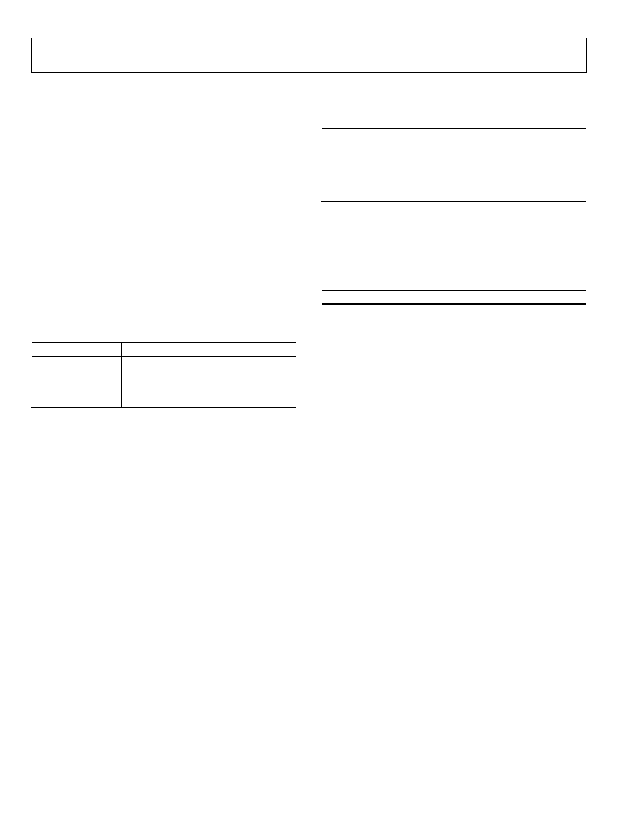
Table 26. Default Register Settings for Clock Distribution Mode
Register
Description
0x010[1:0] = 01b
PLL asynchronous power-down (PLL off)
0x1E0[2:0] = 000b
Set VCO divider = 2
0x1E1[0] = 0b
Use the VCO divider
0x1E1[1] = 0b
Select CLK as the source
When the internal PLL is used with an external VCO, the PLL
must be turned on.
Table 27. Settings When Using an External VCO
Register
Description
0x010[1:0] = 00b
PLL normal operation (PLL on)
0x010 to 0x01E
PLL settings; select and enable a reference
input; set R, N (P, A, B), PFD polarity, and ICP
according to the intended loop configuration
0x1E1[1] = 0b
Select CLK as the source
An external VCO requires an external loop filter that must be
connected between CP and the tuning pin of the VCO. This
loop filter determines the loop bandwidth and stability of the
PLL. Make sure to select the proper PFD polarity for the VCO
being used.
Table 28. Setting the PFD Polarity
Register
Description
0x010[7] = 0b
PFD polarity positive (higher control voltage
produces higher frequency)
0x010[7] = 1b
PFD polarity negative (higher control voltage
produces lower frequency)
相关PDF资料 |
PDF描述 |
|---|---|
| V24A8H300BF2 | CONVERTER MOD DC/DC 8V 300W |
| SY89430VZH TR | IC SYNTHESIZER FREQ PROGR 28SOIC |
| SY89429VJZ TR | IC SYNTHESIZER FREQ PROGR 28PLCC |
| MS3108E28-15SW | CONN PLUG 35POS RT ANG W/SCKT |
| V24A48H300BL | CONVERTER MOD DC/DC 48V 300W |
相关代理商/技术参数 |
参数描述 |
|---|---|
| AD9520-2 | 制造商:AD 制造商全称:Analog Devices 功能描述:12 LVPECL/24 CMOS Output Clock Generator with Integrated 2.2 GHz VCO |
| AD9520-2/PCBZ | 功能描述:BOARD EVAL AD9520-2 RoHS:是 类别:编程器,开发系统 >> 评估演示板和套件 系列:- 标准包装:1 系列:- 主要目的:电信,线路接口单元(LIU) 嵌入式:- 已用 IC / 零件:IDT82V2081 主要属性:T1/J1/E1 LIU 次要属性:- 已供物品:板,电源,线缆,CD 其它名称:82EBV2081 |
| AD9520-2BCPZ | 功能描述:IC CLOCK GEN 2.2GHZ VCO 64LFCSP RoHS:是 类别:集成电路 (IC) >> 时钟/计时 - 时钟发生器,PLL,频率合成器 系列:- 标准包装:2,000 系列:- 类型:PLL 时钟发生器 PLL:带旁路 输入:LVCMOS,LVPECL 输出:LVCMOS 电路数:1 比率 - 输入:输出:2:11 差分 - 输入:输出:是/无 频率 - 最大:240MHz 除法器/乘法器:是/无 电源电压:3.135 V ~ 3.465 V 工作温度:0°C ~ 70°C 安装类型:表面贴装 封装/外壳:32-LQFP 供应商设备封装:32-TQFP(7x7) 包装:带卷 (TR) |
| AD9520-2BCPZ-REEL7 | 功能描述:IC CLOCK GEN 2.2GHZ VCO 64LFCSP RoHS:是 类别:集成电路 (IC) >> 时钟/计时 - 时钟发生器,PLL,频率合成器 系列:- 标准包装:2,000 系列:- 类型:PLL 时钟发生器 PLL:带旁路 输入:LVCMOS,LVPECL 输出:LVCMOS 电路数:1 比率 - 输入:输出:2:11 差分 - 输入:输出:是/无 频率 - 最大:240MHz 除法器/乘法器:是/无 电源电压:3.135 V ~ 3.465 V 工作温度:0°C ~ 70°C 安装类型:表面贴装 封装/外壳:32-LQFP 供应商设备封装:32-TQFP(7x7) 包装:带卷 (TR) |
| AD9520-3 | 制造商:AD 制造商全称:Analog Devices 功能描述:12 LVPECL/24 CMOS Output Clock Generator with Integrated 2 GHz VCO |
发布紧急采购,3分钟左右您将得到回复。