- 您现在的位置:买卖IC网 > PDF目录9085 > AD9520-1BCPZ-REEL7 (Analog Devices Inc)IC CLOCK GEN 2.5GHZ VCO 64LFCSP PDF资料下载
参数资料
| 型号: | AD9520-1BCPZ-REEL7 |
| 厂商: | Analog Devices Inc |
| 文件页数: | 66/80页 |
| 文件大小: | 0K |
| 描述: | IC CLOCK GEN 2.5GHZ VCO 64LFCSP |
| 设计资源: | Synchronizing Multiple AD9910 1 GSPS Direct Digital Synthesizers (CN0121) Phase Coherent FSK Modulator (CN0186) |
| 标准包装: | 750 |
| 类型: | 时钟发生器,扇出配送 |
| PLL: | 是 |
| 输入: | CMOS,LVDS,LVPECL |
| 输出: | CMOS,LVPECL |
| 电路数: | 1 |
| 比率 - 输入:输出: | 2:12,2:24 |
| 差分 - 输入:输出: | 是/是 |
| 频率 - 最大: | 2.65GHz |
| 除法器/乘法器: | 是/无 |
| 电源电压: | 3.135 V ~ 3.465 V |
| 工作温度: | -40°C ~ 85°C |
| 安装类型: | 表面贴装 |
| 封装/外壳: | 64-VFQFN 裸露焊盘,CSP |
| 供应商设备封装: | 64-LFCSP-VQ(9x9) |
| 包装: | 带卷 (TR) |
| 配用: | AD9520-1/PCBZ-ND - BOARD EVAL FOR AD9520-1 |
第1页第2页第3页第4页第5页第6页第7页第8页第9页第10页第11页第12页第13页第14页第15页第16页第17页第18页第19页第20页第21页第22页第23页第24页第25页第26页第27页第28页第29页第30页第31页第32页第33页第34页第35页第36页第37页第38页第39页第40页第41页第42页第43页第44页第45页第46页第47页第48页第49页第50页第51页第52页第53页第54页第55页第56页第57页第58页第59页第60页第61页第62页第63页第64页第65页当前第66页第67页第68页第69页第70页第71页第72页第73页第74页第75页第76页第77页第78页第79页第80页
Data Sheet
AD9520-1
Rev. A | Page 69 of 80
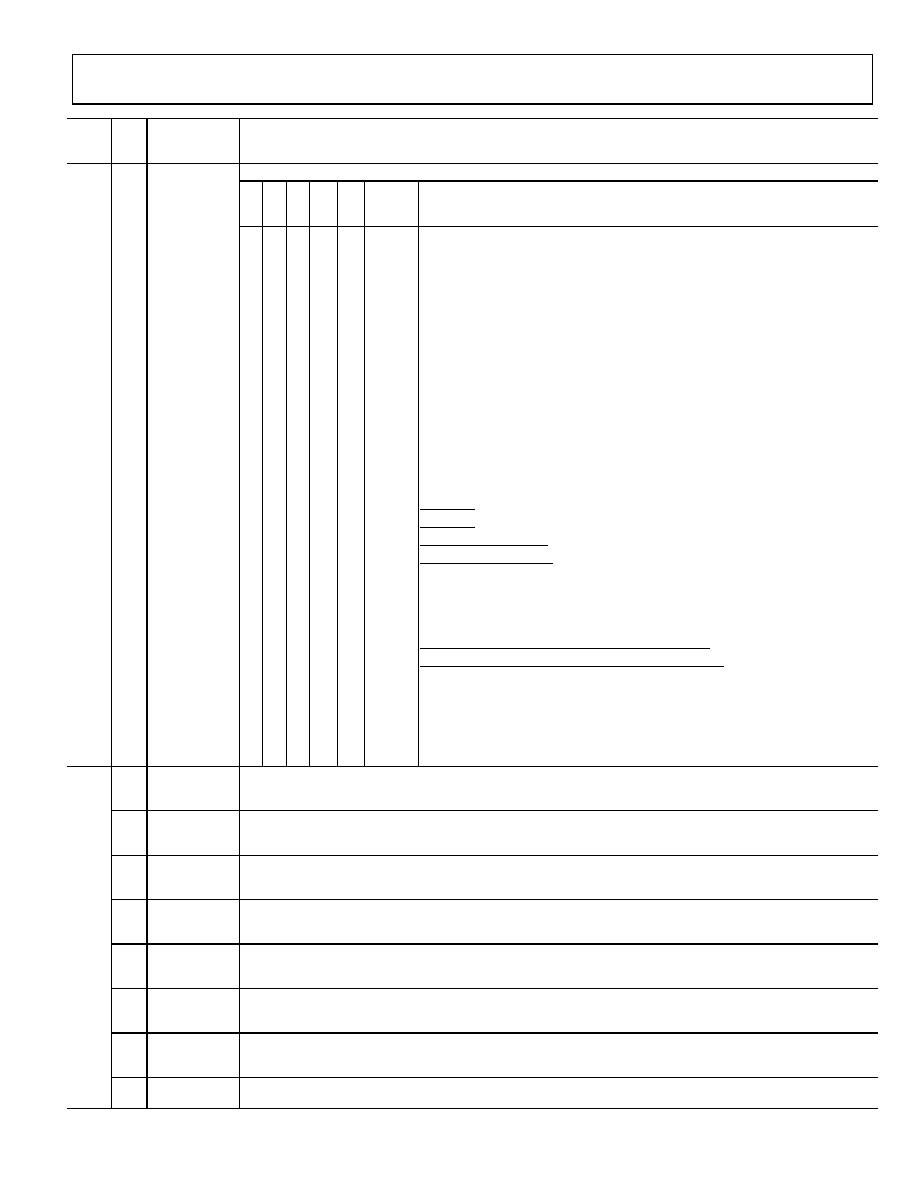
Reg.
Addr.
(Hex)
Bits
Name
Description
[4:0]
REFMON pin
control
Selects the signal that is connected to the REFMON pin.
Bit
4
Bit
3
Bit
2
Bit
1
Bit
0
Level or
Dynamic
Signal
Signal at REFMON Pin
0
LVL
Ground, dc (default).
0
1
DYN
REF1 clock (differential reference when in differential mode).
0
1
0
DYN
REF2 clock (N/A in differential mode).
0
1
DYN
Selected reference to PLL (differential reference when in differential mode).
0
1
0
DYN
Unselected reference to PLL (not available in differential mode).
0
1
0
1
LVL
Status of selected reference (status of differential reference); active high.
0
1
0
LVL
Status of unselected reference (not available in differential mode); active high.
0
1
LVL
Status of REF1 frequency; active high.
0
1
0
LVL
Status of REF2 frequency; active high.
0
1
0
1
LVL
(Status of REF1 frequency) AND (status of REF2 frequency).
0
1
0
1
0
LVL
(DLD) AND (status of selected reference) AND (status of VCO).
0
1
0
1
LVL
Status of VCO frequency; active high.
0
1
0
LVL
Selected reference (low = REF1, high = REF2).
0
1
0
1
LVL
DLD; active high.
0
1
0
LVL
Holdover active; active high.
0
1
LVL
N/A. Do not use.
1
0
LVL
VS (PLL power supply).
1
0
1
DYN
REF1 clock (differential reference when in differential mode).
1
0
1
0
DYN
REF2 clock (not available in differential mode).
1
0
1
DYN
Selected reference to PLL (differential reference when in differential mode).
1
0
1
0
DYN
Unselected reference to PLL (not available when in differential mode).
1
0
1
0
1
LVL
Status of selected reference (status of differential reference); active low.
1
0
1
0
LVL
Status of unselected reference (not available in differential mode); active low.
1
0
1
LVL
Status of REF1 frequency; active low.
1
0
LVL
Status of REF2 frequency; active low.
1
0
1
LVL
(Status of REF1 frequency) AND (status of REF2 frequency).
1
0
1
0
LVL
(DLD) AND (status of selected reference) AND (status of VCO).
1
0
1
LVL
Status of VCO frequency; active low.
1
0
LVL
Selected reference (low = REF2, high = REF1).
1
0
1
LVL
DLD; active low.
1
0
LVL
Holdover active; active low.
1
LVL
N/A. Do not use.
0x01C 7
Disable
switchover
deglitch
Disables or enables the switchover deglitch circuit.
0: enables the switchover deglitch circuit (default).
1: disables the switchover deglitch circuit.
6
Select REF2
If Register 0x01C[5] = 0b, selects the reference for PLL when in manual; register selected reference control.
0: selects REF1 (default).
1: selects REF2.
5
Use REF_SEL pin If Register 0x01C[4] = 0b (manual), sets the method of PLL reference selection.
0: uses Register 0x01C[6] (default).
1: uses REF_SEL pin.
4
Enable automatic
reference
switchover
Automatic or manual reference switchover. Single-ended reference mode must be selected by Register 0x01C[0] = 0b.
0: manual reference switchover (default).
1: automatic reference switchover. Setting this bit also powers on REF1 and REF2 and overrides the settings in Register 0x01C[2:1].
3
Stay on REF2
Stays on REF2 after switchover.
0: returns to REF1 automatically when REF1 status is good again (default).
1: stays on REF2 after switchover. Does not automatically return to REF1.
2
Enable REF2
This bit turns the REF2 power on. This bit is overridden when automatic reference switchover is enabled.
0: REF2 power off (default).
1: REF2 power on.
1
Enable REF1
This bit turns the REF1 power on. This bit is overridden when automatic reference switchover is enabled.
0: REF1 power off (default).
1: REF1 power on.
0
Enable
differential ref
Selects the PLL reference mode, differential or single-ended. Register 0x01C[2:1] should be cleared when this bit is set.
0: single-ended reference mode (default); 1: differential reference mode.
相关PDF资料 |
PDF描述 |
|---|---|
| V24A8H300BF2 | CONVERTER MOD DC/DC 8V 300W |
| SY89430VZH TR | IC SYNTHESIZER FREQ PROGR 28SOIC |
| SY89429VJZ TR | IC SYNTHESIZER FREQ PROGR 28PLCC |
| MS3108E28-15SW | CONN PLUG 35POS RT ANG W/SCKT |
| V24A48H300BL | CONVERTER MOD DC/DC 48V 300W |
相关代理商/技术参数 |
参数描述 |
|---|---|
| AD9520-2 | 制造商:AD 制造商全称:Analog Devices 功能描述:12 LVPECL/24 CMOS Output Clock Generator with Integrated 2.2 GHz VCO |
| AD9520-2/PCBZ | 功能描述:BOARD EVAL AD9520-2 RoHS:是 类别:编程器,开发系统 >> 评估演示板和套件 系列:- 标准包装:1 系列:- 主要目的:电信,线路接口单元(LIU) 嵌入式:- 已用 IC / 零件:IDT82V2081 主要属性:T1/J1/E1 LIU 次要属性:- 已供物品:板,电源,线缆,CD 其它名称:82EBV2081 |
| AD9520-2BCPZ | 功能描述:IC CLOCK GEN 2.2GHZ VCO 64LFCSP RoHS:是 类别:集成电路 (IC) >> 时钟/计时 - 时钟发生器,PLL,频率合成器 系列:- 标准包装:2,000 系列:- 类型:PLL 时钟发生器 PLL:带旁路 输入:LVCMOS,LVPECL 输出:LVCMOS 电路数:1 比率 - 输入:输出:2:11 差分 - 输入:输出:是/无 频率 - 最大:240MHz 除法器/乘法器:是/无 电源电压:3.135 V ~ 3.465 V 工作温度:0°C ~ 70°C 安装类型:表面贴装 封装/外壳:32-LQFP 供应商设备封装:32-TQFP(7x7) 包装:带卷 (TR) |
| AD9520-2BCPZ-REEL7 | 功能描述:IC CLOCK GEN 2.2GHZ VCO 64LFCSP RoHS:是 类别:集成电路 (IC) >> 时钟/计时 - 时钟发生器,PLL,频率合成器 系列:- 标准包装:2,000 系列:- 类型:PLL 时钟发生器 PLL:带旁路 输入:LVCMOS,LVPECL 输出:LVCMOS 电路数:1 比率 - 输入:输出:2:11 差分 - 输入:输出:是/无 频率 - 最大:240MHz 除法器/乘法器:是/无 电源电压:3.135 V ~ 3.465 V 工作温度:0°C ~ 70°C 安装类型:表面贴装 封装/外壳:32-LQFP 供应商设备封装:32-TQFP(7x7) 包装:带卷 (TR) |
| AD9520-3 | 制造商:AD 制造商全称:Analog Devices 功能描述:12 LVPECL/24 CMOS Output Clock Generator with Integrated 2 GHz VCO |
发布紧急采购,3分钟左右您将得到回复。