- 您现在的位置:买卖IC网 > PDF目录9085 > AD9520-1BCPZ-REEL7 (Analog Devices Inc)IC CLOCK GEN 2.5GHZ VCO 64LFCSP PDF资料下载
参数资料
| 型号: | AD9520-1BCPZ-REEL7 |
| 厂商: | Analog Devices Inc |
| 文件页数: | 36/80页 |
| 文件大小: | 0K |
| 描述: | IC CLOCK GEN 2.5GHZ VCO 64LFCSP |
| 设计资源: | Synchronizing Multiple AD9910 1 GSPS Direct Digital Synthesizers (CN0121) Phase Coherent FSK Modulator (CN0186) |
| 标准包装: | 750 |
| 类型: | 时钟发生器,扇出配送 |
| PLL: | 是 |
| 输入: | CMOS,LVDS,LVPECL |
| 输出: | CMOS,LVPECL |
| 电路数: | 1 |
| 比率 - 输入:输出: | 2:12,2:24 |
| 差分 - 输入:输出: | 是/是 |
| 频率 - 最大: | 2.65GHz |
| 除法器/乘法器: | 是/无 |
| 电源电压: | 3.135 V ~ 3.465 V |
| 工作温度: | -40°C ~ 85°C |
| 安装类型: | 表面贴装 |
| 封装/外壳: | 64-VFQFN 裸露焊盘,CSP |
| 供应商设备封装: | 64-LFCSP-VQ(9x9) |
| 包装: | 带卷 (TR) |
| 配用: | AD9520-1/PCBZ-ND - BOARD EVAL FOR AD9520-1 |
第1页第2页第3页第4页第5页第6页第7页第8页第9页第10页第11页第12页第13页第14页第15页第16页第17页第18页第19页第20页第21页第22页第23页第24页第25页第26页第27页第28页第29页第30页第31页第32页第33页第34页第35页当前第36页第37页第38页第39页第40页第41页第42页第43页第44页第45页第46页第47页第48页第49页第50页第51页第52页第53页第54页第55页第56页第57页第58页第59页第60页第61页第62页第63页第64页第65页第66页第67页第68页第69页第70页第71页第72页第73页第74页第75页第76页第77页第78页第79页第80页
Data Sheet
AD9520-1
Rev. A | Page 41 of 80
PROGRAMMABLE
N DELAY
CLK
REF1
REF2
BUF
STATUS
R
DI
V
IDE
R
CL
O
CK
DO
UBL
E
R
VCO STATUS
P
RO
G
RAM
M
ABL
E
R
DE
L
AY
REFERENCE
SWITCHOVER
REF_SEL
CPRSET VCP
VS
GND
RSET
DISTRIBUTION
REFERENCE
REFMON
CP
STATUS
LD
P, P + 1
PRESCALER
A/B
COUNTERS
N DIVIDER
BYPASS
LF
LOW DROPOUT
REGULATOR (LDO)
PHASE
FREQUENCY
DETECTOR
LOCK
DETECT
CHARGE
PUMP
PL
L
RE
F
E
RE
NCE
HOLD
0
1
DIVIDE BY 1,
2, 3, 4, 5, OR 6
ZERO DELAY BLOCK
FROM CHANNEL
DIVIDER 0
VS_DRV
REFIN
OPTIONAL
REFIN
07214-
070
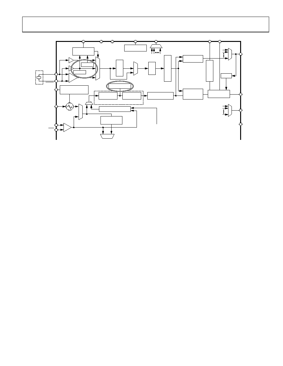
Figure 48. Reference and VCO/CLK Frequency Status Monitors
Frequency Status Monitors
The AD9520 contains three frequency status monitors that are
used to indicate if the PLL reference (or references, in the case of
single-ended mode) and the VCO/CLK input have fallen below
a threshold frequency. Note that the VCO frequency monitor
becomes a CLK input frequency monitor if the CLK input is
selected instead of the internal VCO. Figure 48 shows the
location of the frequency status monitors in the PLL.
The PLL reference monitors have two threshold frequencies:
normal and extended (see Table 17). The reference frequency
monitor thresholds are set in Register 0x01A[6].
VCO Calibration
The AD9520 on-chip VCO must be calibrated to ensure proper
operation over process and temperature. The VCO calibration
is controlled by a calibration controller running off a divided
REFIN clock. The calibration requires that the PLL be set up
properly to lock the PLL loop and that the REFIN clock be
present. The REFIN clock must come from a stable source
external to the AD9520.
VCO calibration can be performed two ways: automatically at
power-up and manually. Automatic VCO calibration occurs when
the EEPROM is set to automatically load the preprogrammed
values in the EEPROM and then automatically calibrate the VCO.
For the automatic calibration to complete, a valid reference must
be provided at power-up. If no valid reference is provided, the
user must calibrate the VCO manually.
During the first initialization after a power-up or a reset of
the AD9520, a manual VCO calibration sequence is initiated
by setting Register 0x018[0] = 1b. This can be done as part of
the initial setup before executing an update all registers operation
(IO_UPDATE, Register 0x232[0] = 1b).
Subsequent to the initial setup, a VCO calibration sequence
is initiated by resetting Register 0x018[0] = 0b, executing an
IO_UPDATE, setting Register 0x018[0] = 1b, and executing
another IO_UPDATE. A readback bit (Register 0x01F[6])
indicates when VCO calibration is finished by returning a logic
true (that is, 1b).
The sequence of operations for the VCO calibration follows:
1. Program the PLL registers to the proper values for the PLL
loop. Note that the VCO divider (Register 0x1E0[2:0])
must not be set to static during VCO calibration.
2. Ensure that the input reference signal is present.
3. For initial setting of the registers after a power-up or reset,
initiate a VCO calibration by setting Register 0x018[0] = 1b.
4. Subsequently, whenever a calibration is desired, set
Register 0x018[0] = 0b, update registers; and then set
Register 0x018[0] = 1b, update registers.
5. A SYNC operation is initiated internally, causing the outputs
to go to a static state determined by normal SYNC function
operation.
6. VCO is calibrated to the desired setting for the requested
VCO frequency.
7. Internally, the SYNC signal is released, allowing outputs to
continue clocking.
8. The PLL loop is closed.
9. The PLL locks.
A SYNC is executed during the VCO calibration; therefore, the
outputs of the AD9520 are held static during the calibration, which
prevents unwanted frequencies from being produced. However,
at the end of a VCO calibration, the outputs may resume clocking
before the PLL loop is completely settled.
相关PDF资料 |
PDF描述 |
|---|---|
| V24A8H300BF2 | CONVERTER MOD DC/DC 8V 300W |
| SY89430VZH TR | IC SYNTHESIZER FREQ PROGR 28SOIC |
| SY89429VJZ TR | IC SYNTHESIZER FREQ PROGR 28PLCC |
| MS3108E28-15SW | CONN PLUG 35POS RT ANG W/SCKT |
| V24A48H300BL | CONVERTER MOD DC/DC 48V 300W |
相关代理商/技术参数 |
参数描述 |
|---|---|
| AD9520-2 | 制造商:AD 制造商全称:Analog Devices 功能描述:12 LVPECL/24 CMOS Output Clock Generator with Integrated 2.2 GHz VCO |
| AD9520-2/PCBZ | 功能描述:BOARD EVAL AD9520-2 RoHS:是 类别:编程器,开发系统 >> 评估演示板和套件 系列:- 标准包装:1 系列:- 主要目的:电信,线路接口单元(LIU) 嵌入式:- 已用 IC / 零件:IDT82V2081 主要属性:T1/J1/E1 LIU 次要属性:- 已供物品:板,电源,线缆,CD 其它名称:82EBV2081 |
| AD9520-2BCPZ | 功能描述:IC CLOCK GEN 2.2GHZ VCO 64LFCSP RoHS:是 类别:集成电路 (IC) >> 时钟/计时 - 时钟发生器,PLL,频率合成器 系列:- 标准包装:2,000 系列:- 类型:PLL 时钟发生器 PLL:带旁路 输入:LVCMOS,LVPECL 输出:LVCMOS 电路数:1 比率 - 输入:输出:2:11 差分 - 输入:输出:是/无 频率 - 最大:240MHz 除法器/乘法器:是/无 电源电压:3.135 V ~ 3.465 V 工作温度:0°C ~ 70°C 安装类型:表面贴装 封装/外壳:32-LQFP 供应商设备封装:32-TQFP(7x7) 包装:带卷 (TR) |
| AD9520-2BCPZ-REEL7 | 功能描述:IC CLOCK GEN 2.2GHZ VCO 64LFCSP RoHS:是 类别:集成电路 (IC) >> 时钟/计时 - 时钟发生器,PLL,频率合成器 系列:- 标准包装:2,000 系列:- 类型:PLL 时钟发生器 PLL:带旁路 输入:LVCMOS,LVPECL 输出:LVCMOS 电路数:1 比率 - 输入:输出:2:11 差分 - 输入:输出:是/无 频率 - 最大:240MHz 除法器/乘法器:是/无 电源电压:3.135 V ~ 3.465 V 工作温度:0°C ~ 70°C 安装类型:表面贴装 封装/外壳:32-LQFP 供应商设备封装:32-TQFP(7x7) 包装:带卷 (TR) |
| AD9520-3 | 制造商:AD 制造商全称:Analog Devices 功能描述:12 LVPECL/24 CMOS Output Clock Generator with Integrated 2 GHz VCO |
发布紧急采购,3分钟左右您将得到回复。