- 您现在的位置:买卖IC网 > PDF目录9085 > AD9520-1BCPZ-REEL7 (Analog Devices Inc)IC CLOCK GEN 2.5GHZ VCO 64LFCSP PDF资料下载
参数资料
| 型号: | AD9520-1BCPZ-REEL7 |
| 厂商: | Analog Devices Inc |
| 文件页数: | 32/80页 |
| 文件大小: | 0K |
| 描述: | IC CLOCK GEN 2.5GHZ VCO 64LFCSP |
| 设计资源: | Synchronizing Multiple AD9910 1 GSPS Direct Digital Synthesizers (CN0121) Phase Coherent FSK Modulator (CN0186) |
| 标准包装: | 750 |
| 类型: | 时钟发生器,扇出配送 |
| PLL: | 是 |
| 输入: | CMOS,LVDS,LVPECL |
| 输出: | CMOS,LVPECL |
| 电路数: | 1 |
| 比率 - 输入:输出: | 2:12,2:24 |
| 差分 - 输入:输出: | 是/是 |
| 频率 - 最大: | 2.65GHz |
| 除法器/乘法器: | 是/无 |
| 电源电压: | 3.135 V ~ 3.465 V |
| 工作温度: | -40°C ~ 85°C |
| 安装类型: | 表面贴装 |
| 封装/外壳: | 64-VFQFN 裸露焊盘,CSP |
| 供应商设备封装: | 64-LFCSP-VQ(9x9) |
| 包装: | 带卷 (TR) |
| 配用: | AD9520-1/PCBZ-ND - BOARD EVAL FOR AD9520-1 |
第1页第2页第3页第4页第5页第6页第7页第8页第9页第10页第11页第12页第13页第14页第15页第16页第17页第18页第19页第20页第21页第22页第23页第24页第25页第26页第27页第28页第29页第30页第31页当前第32页第33页第34页第35页第36页第37页第38页第39页第40页第41页第42页第43页第44页第45页第46页第47页第48页第49页第50页第51页第52页第53页第54页第55页第56页第57页第58页第59页第60页第61页第62页第63页第64页第65页第66页第67页第68页第69页第70页第71页第72页第73页第74页第75页第76页第77页第78页第79页第80页
AD9520-1
Data Sheet
Rev. A | Page 38 of 80
Digital Lock Detect (DLD)
By selecting the proper output through the mux on each pin, the
DLD function is available at the LD, STATUS, and REFMON pins.
The digital lock detect circuit indicates a lock when the time
difference of the rising edges at the PFD inputs is less than a
specified value (the lock threshold). The loss of a lock is indicated
when the time difference exceeds a specified value (the unlock
threshold). Note that the unlock threshold is wider than the
lock threshold, which allows some phase error in excess of the
lock window to occur without chattering on the lock indicator.
The lock detect window timing depends on the value of the
CPRSET resistor, as well as three settings: the digital lock
detect window bit (Register 0x018[4]), the antibacklash pulse
width bit (Register 0x017[1:0], see Table 2), and the lock detect
counter (Register 0x018[6:5]). The lock and unlock detection
5.11 kΩ. Doubling the CPRSET value to 10 kΩ doubles the
values in Table 2.
A lock is not indicated until there is a programmable number of
consecutive PFD cycles with a time difference that is less than the
lock detect threshold. The lock detect circuit continues to indicate
a lock until a time difference that is greater than the unlock
threshold occurs on a single subsequent cycle. For the lock detect
to work properly, the period of the PFD frequency must be
greater than the unlock threshold. The number of consecutive PFD
cycles required for lock is programmable (Register 0x018[6:5]).
Note that, in certain low (<500 Hz) loop bandwidth, high phase
margin cases, the DLD may chatter during acquisition, which
can cause the AD9520 to automatically enter and exit holdover.
To avoid this problem, it is recommended that the user provide
for a capacitor to ground on the LD pin such that current source
digital lock detect (CSDLD) mode can be used.
Analog Lock Detect (ALD)
The AD9520 provides an ALD function that can be selected for
use at the LD pin. There are two operating modes for ALD:
N-channel open-drain lock detect. This signal requires a
pull-up resistor to the positive supply, VS. The output is
normally high with short, low going pulses. Lock is
indicated by the minimum duty cycle of the low going pulses.
P-channel open-drain lock detect. This signal requires a
pull-down resistor to GND. The output is normally low with
short, high going pulses. Lock is indicated by the minimum
duty cycle of the high going pulses.
AD9520
ALD
LD
R1
C
VOUT
R2
VS = 3.3V
07214-
067
Figure 44. Example of Analog Lock Detect Filter Using
N-Channel Open-Drain Driver
The analog lock detect function requires an RC filter to provide a
logic level indicating lock/unlock. The ADIsimCLK tool can be
used to help the user select the right passive component values
for ALD to ensure its correct operation.
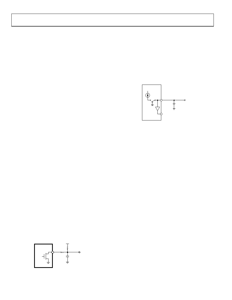
Current Source Digital Lock Detect (CSDLD)
During the PLL locking sequence, it is normal for the DLD
signal to toggle a number of times before remaining steady
when the PLL is completely locked and stable. There may be
applications where it is desirable to have DLD asserted only
after the PLL is solidly locked. This is possible by using the
current source digital lock detect function.
AD9520
LD
REFMON
OR
STATUS
C
VOUT
110A
DLD
LD PIN
COMPARATOR
07214-
068
Figure 45. Current Source Digital Lock Detect
The current source lock detect provides a current of 110 A when
DLD is true and shorts to ground when DLD is false. If a capacitor
is connected to the LD pin, it charges at a rate determined by the
current source during the DLD true time but is discharged nearly
instantly when DLD is false. By monitoring the voltage at the
LD pin (top of the capacitor), LD = high happens only after the
DLD is true for a sufficiently long time. Any momentary DLD
false resets the charging. By selecting a properly sized capacitor,
it is possible to delay a lock detect indication until the PLL is
stably locked and the lock detect does not chatter.
To use current source digital lock detect, do the following:
Place a capacitor to ground on the LD pin.
Set Register 0x01A[5:0] = 0x04.
Enable the LD pin comparator (Register 0x01D[3] = 1b).
The LD pin comparator senses the voltage on the LD pin, and the
comparator output can be made available at the REFMON pin
control (Register 0x01B[4:0]) or the STATUS pin control (Register
0x017[7:2]). The internal LD pin comparator trip point and
hysteresis are given in Table 17. The voltage on the capacitor can
also be sensed by an external comparator that is connected to
the LD pin. In this case, enabling the on-board LD pin comparator
is not necessary.
The user can asynchronously enable individual clock outputs only
when CSDLD is high. To enable this feature, set the appropriate bits
in the enable output on the CSDLD registers (Register 0x0FC and
Register0x0FD).
相关PDF资料 |
PDF描述 |
|---|---|
| V24A8H300BF2 | CONVERTER MOD DC/DC 8V 300W |
| SY89430VZH TR | IC SYNTHESIZER FREQ PROGR 28SOIC |
| SY89429VJZ TR | IC SYNTHESIZER FREQ PROGR 28PLCC |
| MS3108E28-15SW | CONN PLUG 35POS RT ANG W/SCKT |
| V24A48H300BL | CONVERTER MOD DC/DC 48V 300W |
相关代理商/技术参数 |
参数描述 |
|---|---|
| AD9520-2 | 制造商:AD 制造商全称:Analog Devices 功能描述:12 LVPECL/24 CMOS Output Clock Generator with Integrated 2.2 GHz VCO |
| AD9520-2/PCBZ | 功能描述:BOARD EVAL AD9520-2 RoHS:是 类别:编程器,开发系统 >> 评估演示板和套件 系列:- 标准包装:1 系列:- 主要目的:电信,线路接口单元(LIU) 嵌入式:- 已用 IC / 零件:IDT82V2081 主要属性:T1/J1/E1 LIU 次要属性:- 已供物品:板,电源,线缆,CD 其它名称:82EBV2081 |
| AD9520-2BCPZ | 功能描述:IC CLOCK GEN 2.2GHZ VCO 64LFCSP RoHS:是 类别:集成电路 (IC) >> 时钟/计时 - 时钟发生器,PLL,频率合成器 系列:- 标准包装:2,000 系列:- 类型:PLL 时钟发生器 PLL:带旁路 输入:LVCMOS,LVPECL 输出:LVCMOS 电路数:1 比率 - 输入:输出:2:11 差分 - 输入:输出:是/无 频率 - 最大:240MHz 除法器/乘法器:是/无 电源电压:3.135 V ~ 3.465 V 工作温度:0°C ~ 70°C 安装类型:表面贴装 封装/外壳:32-LQFP 供应商设备封装:32-TQFP(7x7) 包装:带卷 (TR) |
| AD9520-2BCPZ-REEL7 | 功能描述:IC CLOCK GEN 2.2GHZ VCO 64LFCSP RoHS:是 类别:集成电路 (IC) >> 时钟/计时 - 时钟发生器,PLL,频率合成器 系列:- 标准包装:2,000 系列:- 类型:PLL 时钟发生器 PLL:带旁路 输入:LVCMOS,LVPECL 输出:LVCMOS 电路数:1 比率 - 输入:输出:2:11 差分 - 输入:输出:是/无 频率 - 最大:240MHz 除法器/乘法器:是/无 电源电压:3.135 V ~ 3.465 V 工作温度:0°C ~ 70°C 安装类型:表面贴装 封装/外壳:32-LQFP 供应商设备封装:32-TQFP(7x7) 包装:带卷 (TR) |
| AD9520-3 | 制造商:AD 制造商全称:Analog Devices 功能描述:12 LVPECL/24 CMOS Output Clock Generator with Integrated 2 GHz VCO |
发布紧急采购,3分钟左右您将得到回复。