- 您现在的位置:买卖IC网 > PDF目录16848 > AD9524/PCBZ (Analog Devices Inc)BOARD EVAL FOR AD9524 PDF资料下载
参数资料
| 型号: | AD9524/PCBZ |
| 厂商: | Analog Devices Inc |
| 文件页数: | 16/56页 |
| 文件大小: | 0K |
| 描述: | BOARD EVAL FOR AD9524 |
| 设计资源: | AD9524 Schematic AD9524 BOM AD9524 Gerber Files |
| 标准包装: | 1 |
| 主要目的: | 计时,时钟发生器 |
| 嵌入式: | 否 |
| 已用 IC / 零件: | AD9524 |
| 主要属性: | USB 供电或外部电源 |
| 次要属性: | 状态 LED |
| 已供物品: | 板 |
| 配用: | AD9524BCPZ-ND - IC INTEGER-N CLCK GEN 48LFCSP |
第1页第2页第3页第4页第5页第6页第7页第8页第9页第10页第11页第12页第13页第14页第15页当前第16页第17页第18页第19页第20页第21页第22页第23页第24页第25页第26页第27页第28页第29页第30页第31页第32页第33页第34页第35页第36页第37页第38页第39页第40页第41页第42页第43页第44页第45页第46页第47页第48页第49页第50页第51页第52页第53页第54页第55页第56页
Data Sheet
AD9524
Rev. E | Page 23 of 56
CLOCK DISTRIBUTION
The clock distribution block provides an integrated solution for
generating multiple clock outputs based on frequency dividing
the PLL2 VCO divider output. The distribution output consists
of six channels (OUT0 to OUT5). Each of the output channels
has a dedicated divider and output driver, as shown in Figure 25.
The AD9524 also has the capability to route the VCXO output
to two of the outputs (OUT0 and OUT1).
Clock Dividers
The output clock distribution dividers are referred to as D0 to D5,
corresponding to output channels OUT0 through OUT5,
respectively. Each divider is programmable with 10 bits of division
depth that is equal to 1 to 1024. Dividers have duty cycle correction
to always give 50% duty cycle, even for odd divides.
Output Power-Down
Each of the output channels offers independent control of the
power-down functionality via the Channel 0 to Channel 5 control
registers (see Table 52). Each output channel has a dedicated
power-down bit for powering down the output driver. However,
if all six outputs are powered down, the entire distribution output
enters a deep sleep mode. Although each channel has a channel
power-down control signal, it may sometimes be desirable to
power down an output driver while maintaining the divider’s
synchronization with the other channel dividers. This is accom-
plished by placing the output in tristate mode (this works in
CMOS mode, as well).
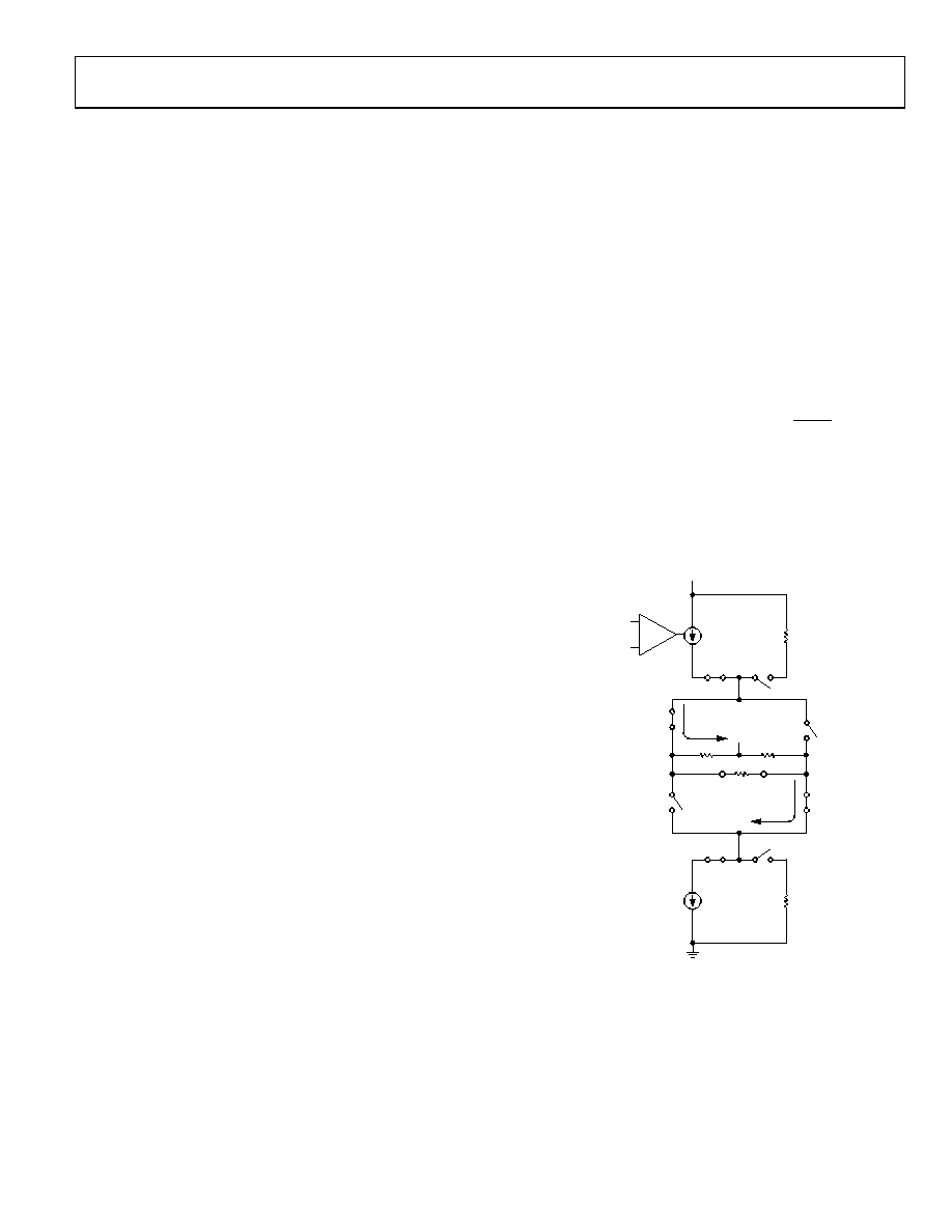
Multimode Output Drivers
The user has independent control of the operating mode of each of
the fourteen output channels via the Channel 0 to Channel 5
control registers (see Table 52). The operating mode control
includes the following:
Logic family and pin functionality
Output drive strength
Output polarity
The four least significant bits (LSBs) of each of the six Channel 0 to
Channel 5 control registers comprise the driver mode bits. The
mode value selects the desired logic family and pin functionality
of an output channel, as listed in Table 52. This driver design
allows a common 100 external resistor for all the different
driver modes of operation that are illustrated in Figure 26.
If the output channel is ac-coupled to the circuit to be clocked,
changing the mode varies the voltage swing to determine sensi-
tivity to the drive level. For example, in LVDS mode, a current of
3.5 mA causes a 350 mV peak voltage. Likewise, in LVPECL
compatible mode, a current of 8 mA causes an 800 mV peak
voltage at the 100 load resistor. Using any termination other
than those specified in the Input/Output Termination
Recommendations section may results in damage or decrease
end of life performance.
In addition to the four mode bits, each of the six Channel 0 to
Channel 5 control registers includes the following control bits:
Invert divider output. Enables the user to choose between
normal polarity and inverted polarity. Normal polarity is the
default state. Inverted polarity reverses the representation of
Logic 0 and Logic 1, regardless of the logic family.
Ignore sync. Makes the divider ignore the SYNC signal
from any source.
Power-down channel. Powers down the entire channel.
Lower power mode.
Driver mode.
Channel divider.
Divider phase.
3.5mA/8mA
LVDS/LVPECL
ENABLED
HSTL
ENABLED
HSTL
ENABLED
50
P
N
P
100 LOAD
CM
VDD3_OUT[x:y]
1.25V LVDS
VDD – 1.3V LVPECL
CM
COMMON-MODE
CIRCUIT
+
–
08439-
031
Figure 26. Multimode Driver
相关PDF资料 |
PDF描述 |
|---|---|
| V150C12E150BF | CONVERTER MOD DC/DC 12V 150W |
| 0982660986 | CBL 27PS 0.5MM JMPR TYPE D 1.18" |
| H6MMH-3006G | DIP CABLE - HDM30H/AE30G/HDM30H |
| TCMD-25-T-02.00-01-N | CABLE ASSEM 2MM 50POS M-F 2" |
| GEC17DRXI-S734 | CONN EDGECARD 34POS DIP .100 SLD |
相关代理商/技术参数 |
参数描述 |
|---|---|
| AD9525 | 制造商:AD 制造商全称:Analog Devices 功能描述:Low Jitter Clock Generator with Eight LVPECL Outputs |
| AD9525/PCBZ | 功能描述:时钟和定时器开发工具 Evaluation kit 2950MHz VCO installed RoHS:否 制造商:Texas Instruments 产品:Evaluation Modules 类型:Clock Conditioners 工具用于评估:LMK04100B 频率:122.8 MHz 工作电源电压:3.3 V |
| AD9525/PCBZ-VCO | 功能描述:时钟和定时器开发工具 Evaluation kit CRO29508 VCO installed RoHS:否 制造商:Texas Instruments 产品:Evaluation Modules 类型:Clock Conditioners 工具用于评估:LMK04100B 频率:122.8 MHz 工作电源电压:3.3 V |
| AD9525BCPZ | 功能描述:时钟发生器及支持产品 High performance clock distributor Exter RoHS:否 制造商:Silicon Labs 类型:Clock Generators 最大输入频率:14.318 MHz 最大输出频率:166 MHz 输出端数量:16 占空比 - 最大:55 % 工作电源电压:3.3 V 工作电源电流:1 mA 最大工作温度:+ 85 C 安装风格:SMD/SMT 封装 / 箱体:QFN-56 |
| AD9525BCPZ-REEL7 | 功能描述:时钟发生器及支持产品 High performance clock distributor Exter RoHS:否 制造商:Silicon Labs 类型:Clock Generators 最大输入频率:14.318 MHz 最大输出频率:166 MHz 输出端数量:16 占空比 - 最大:55 % 工作电源电压:3.3 V 工作电源电流:1 mA 最大工作温度:+ 85 C 安装风格:SMD/SMT 封装 / 箱体:QFN-56 |
发布紧急采购,3分钟左右您将得到回复。