- 您现在的位置:买卖IC网 > PDF目录16848 > AD9524/PCBZ (Analog Devices Inc)BOARD EVAL FOR AD9524 PDF资料下载
参数资料
| 型号: | AD9524/PCBZ |
| 厂商: | Analog Devices Inc |
| 文件页数: | 42/56页 |
| 文件大小: | 0K |
| 描述: | BOARD EVAL FOR AD9524 |
| 设计资源: | AD9524 Schematic AD9524 BOM AD9524 Gerber Files |
| 标准包装: | 1 |
| 主要目的: | 计时,时钟发生器 |
| 嵌入式: | 否 |
| 已用 IC / 零件: | AD9524 |
| 主要属性: | USB 供电或外部电源 |
| 次要属性: | 状态 LED |
| 已供物品: | 板 |
| 配用: | AD9524BCPZ-ND - IC INTEGER-N CLCK GEN 48LFCSP |
第1页第2页第3页第4页第5页第6页第7页第8页第9页第10页第11页第12页第13页第14页第15页第16页第17页第18页第19页第20页第21页第22页第23页第24页第25页第26页第27页第28页第29页第30页第31页第32页第33页第34页第35页第36页第37页第38页第39页第40页第41页当前第42页第43页第44页第45页第46页第47页第48页第49页第50页第51页第52页第53页第54页第55页第56页
Data Sheet
AD9524
Rev. E | Page 47 of 56
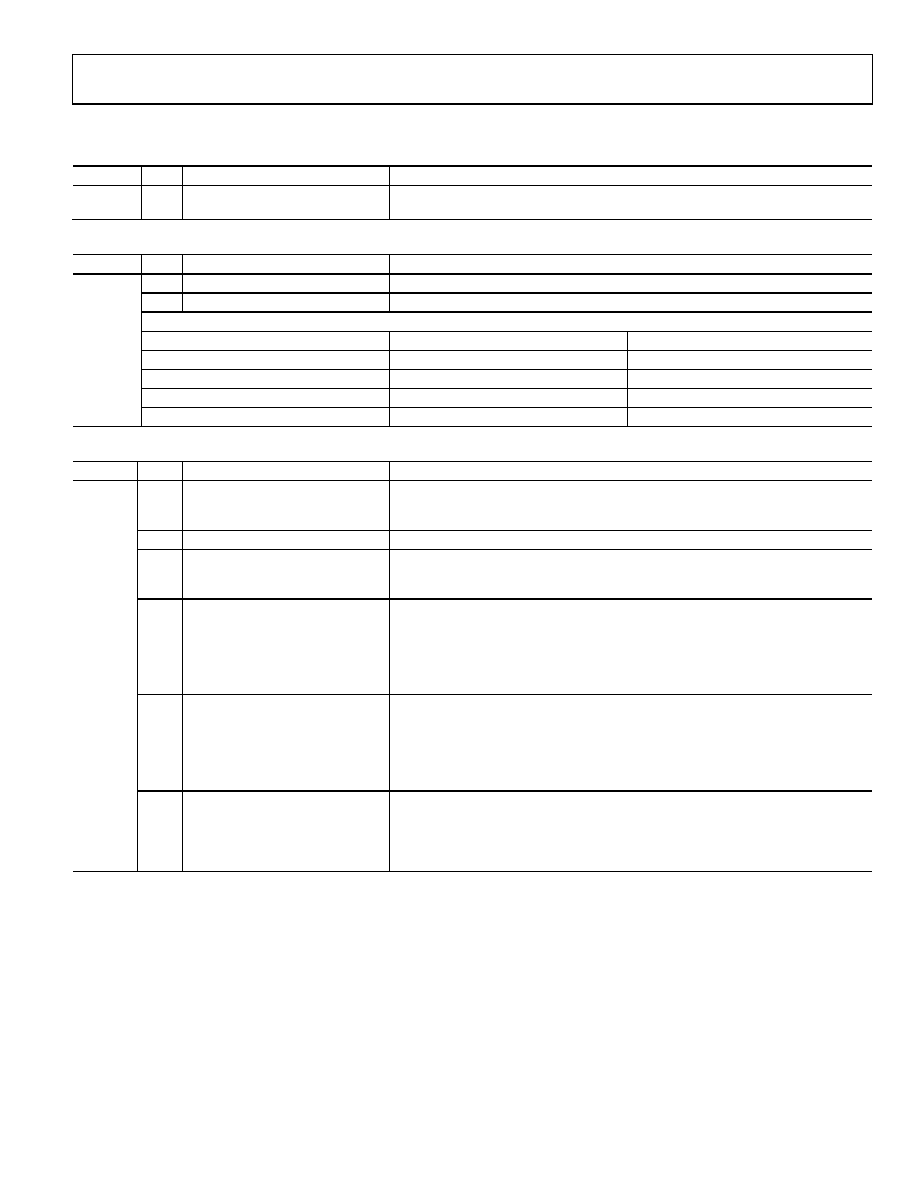
Output PLL (PLL2) (Address 0x0F0 to Address 0x0F9)
Table 45. PLL2 Charge Pump Control
Table 46. PLL2 Feedback N Divider Control
Table 47. PLL2 Control
Address
Bits
Bit Name
Description
0x0F2
7
PLL2 lock detector power-down
Controls power-down of the PLL2 lock detector.
1: lock detector powered down.
0: lock detector active.
6
Reserved
Default = 0; value must remain 0.
5
Enable frequency doubler
Enables doubling of the PLL2 reference input frequency.
1: enabled.
0: disabled.
4
Enable SPI control of antibacklash
pulse width
Controls the functionality of Register 0x0F2, Bits[3:2]. Set the antibacklash pulse
width to the minimum setting. By setting Bit 4 to 1 from the default of 0, Bits[3:2]
consequently default to 00.
0 (default): device automatically controls the antibacklash period to high
(equivalent to Register 0x0F2, Bits[3:2] = 10).
1: antibacklash period defined by Register 0x0F2, Bits[2:1] (recommended setting).
[3:2]
Antibacklash pulse width control
Controls the PFD antibacklash period of PLL2.
00 (default): minimum (recommended setting).
01: low.
10: high.
11: maximum.
These bits are ineffective unless Register 0x0F2, Bit 4 = 1.
[1:0]
PLL2 charge pump mode
Controls the mode of the PLL2 charge pump.
00: tristate.
01: pump up.
10: pump down.
11 (default): normal.
Address
Bits
Bit Name
Description
0x0F0
[7:0]
PLL2 charge pump control
These bits set the magnitude of the PLL2 charge pump current. Granularity is ~3.5 μA
with a full-scale magnitude of ~900 μA.
Address
Bits
Bit Name
Description
0x0F1
[7:6]
A counter
A counter word
[5:0]
B counter
B counter word
Feedback Divider Constraints
A Counter (Bits[7:6])
B Counter (Bits[5:0])
Allowed N Division (4 × B + A)
A = 0 or A = 1
B = 4
16, 17
A = 0 to A = 2
B = 5
20, 21, 22
A = 0 to A = 2
B = 6
24, 25, 26
A = 0 to A = 3
B ≥ 7
28, 29 … continuous to 255
相关PDF资料 |
PDF描述 |
|---|---|
| V150C12E150BF | CONVERTER MOD DC/DC 12V 150W |
| 0982660986 | CBL 27PS 0.5MM JMPR TYPE D 1.18" |
| H6MMH-3006G | DIP CABLE - HDM30H/AE30G/HDM30H |
| TCMD-25-T-02.00-01-N | CABLE ASSEM 2MM 50POS M-F 2" |
| GEC17DRXI-S734 | CONN EDGECARD 34POS DIP .100 SLD |
相关代理商/技术参数 |
参数描述 |
|---|---|
| AD9525 | 制造商:AD 制造商全称:Analog Devices 功能描述:Low Jitter Clock Generator with Eight LVPECL Outputs |
| AD9525/PCBZ | 功能描述:时钟和定时器开发工具 Evaluation kit 2950MHz VCO installed RoHS:否 制造商:Texas Instruments 产品:Evaluation Modules 类型:Clock Conditioners 工具用于评估:LMK04100B 频率:122.8 MHz 工作电源电压:3.3 V |
| AD9525/PCBZ-VCO | 功能描述:时钟和定时器开发工具 Evaluation kit CRO29508 VCO installed RoHS:否 制造商:Texas Instruments 产品:Evaluation Modules 类型:Clock Conditioners 工具用于评估:LMK04100B 频率:122.8 MHz 工作电源电压:3.3 V |
| AD9525BCPZ | 功能描述:时钟发生器及支持产品 High performance clock distributor Exter RoHS:否 制造商:Silicon Labs 类型:Clock Generators 最大输入频率:14.318 MHz 最大输出频率:166 MHz 输出端数量:16 占空比 - 最大:55 % 工作电源电压:3.3 V 工作电源电流:1 mA 最大工作温度:+ 85 C 安装风格:SMD/SMT 封装 / 箱体:QFN-56 |
| AD9525BCPZ-REEL7 | 功能描述:时钟发生器及支持产品 High performance clock distributor Exter RoHS:否 制造商:Silicon Labs 类型:Clock Generators 最大输入频率:14.318 MHz 最大输出频率:166 MHz 输出端数量:16 占空比 - 最大:55 % 工作电源电压:3.3 V 工作电源电流:1 mA 最大工作温度:+ 85 C 安装风格:SMD/SMT 封装 / 箱体:QFN-56 |
发布紧急采购,3分钟左右您将得到回复。