参数资料
| 型号: | AD9577BCPZ-RL |
| 厂商: | Analog Devices Inc |
| 文件页数: | 25/44页 |
| 文件大小: | 0K |
| 描述: | IC CLK GEN PLL DUAL 40LFCSP |
| 标准包装: | 2,500 |
| 系列: | PCI Express® (PCIe) |
| 类型: | 扇出缓冲器(分配),网络时钟发生器,多路复用器 |
| PLL: | 是 |
| 主要目的: | 以太网,PCI Express(PCIe),SONET/SDH |
| 输入: | 时钟,晶体 |
| 输出: | LVCMOS,LVDS,LVPECL |
| 电路数: | 1 |
| 比率 - 输入:输出: | 2:5 |
| 差分 - 输入:输出: | 无/是 |
| 频率 - 最大: | 637.5MHz |
| 电源电压: | 3 V ~ 3.6 V |
| 工作温度: | -40°C ~ 85°C |
| 安装类型: | 表面贴装 |
| 封装/外壳: | 40-WFQFN 裸露焊盘,CSP |
| 供应商设备封装: | 40-LFCSP-WQ(6x6) |
| 包装: | 带卷 (TR) |
第1页第2页第3页第4页第5页第6页第7页第8页第9页第10页第11页第12页第13页第14页第15页第16页第17页第18页第19页第20页第21页第22页第23页第24页当前第25页第26页第27页第28页第29页第30页第31页第32页第33页第34页第35页第36页第37页第38页第39页第40页第41页第42页第43页第44页
Data Sheet
AD9577
Rev. 0 | Page 31 of 44
Table 21.PLL2 Output Driver Format Control Bits,
Register DR1[5:3]
FORMAT2 (PLL2)
Register DR1[5:3]
OUT3P/OUT3N
OUT2P/OUT2N
000
LVPECL
001
LVDS
010
2 × CMOS
LVPECL
011
2 × CMOS
100
2 × CMOS
LVDS
101
LVPECL
LVDS
110
LVPECL
2 × CMOS
2 × CMOS
1 This indicates that the CMOS outputs are in phase; otherwise, they are in
antiphase.
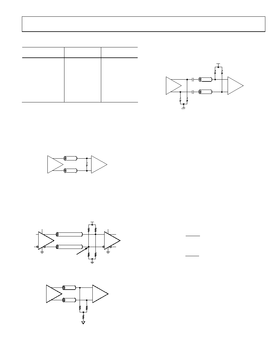
LVDS uses a current mode output stage. The normal value
(default) for this current is 3.5 mA, which yields a 350 mV
output swing across a 100 Ω resistor. The LVDS outputs meet or
exceed all ANSI/TIA/EIA-644 specifications. The LVDS output
buffer should be terminated with a 100 Ω differential resistor
between the receiver input ports (see Figure 38). A recommended
termination circuit for the LVDS outputs is shown in Figure 38.
50
LVDS
100
LVDS
092
84-
042
Figure 38. LVDS Output Termination
See the AN-586 Application Note, LVDS Outputs for High Speed
A/D Converters, for more information about LVDS.
In a dc-coupled application, the LVPECL output buffer should
be terminated via a pair of 50 Ω resistors to a voltage of VCC 2 V.
This can be implemented by using potential dividers of 127 Ω
and 83 Ω between the supplies, as shown in Figure 39.
3.3V
50
SINGLE-ENDED
(NOT COUPLED)
3.3V
LVPECL
127
83
VT = VDD – 2V
LVPECL
0
928
4-
0
43
Figure 39. LVPECL DC-Coupled Termination
An alternative LVPECL termination scheme for dc-coupled
applications is shown Figure 40.
50
LVPECL
50
LVPECL
0
928
4-
0
44
Figure 40. LVPECL DC-Coupled Y-Termination
In ac-coupled applications, the LVPECL output stage needs a
pair of 200 Ω pull-down resistors to GND to provide a dc path for
the output stage emitter followers (see Figure 41). The receiver must
provide an additional 50 Ω single-ended input termination.
50
LVPECL
50
200
LVPECL
VTERM
0.1F
09
284
-045
Figure 41. LVPECL AC-Coupled Termination
REFERENCE OUTPUT BUFFER
A CMOS buffered copy of the reference input circuit signal is
available at the REFOUT pin. This buffer can be optionally
powered down by setting Register DR2[0], PDRefOut to Logic 0.
PLL1 INTEGER-N PLL
The upper PLL in Figure 32, PLL1, is an integer-N PLL with a
loop bandwidth of 140 kHz. The input frequency to the PLL
from the reference circuit is fPFD. The VCO frequency, fVCO1, is
programmed by setting the value for Na, according to
fVCO1 = fPFD × Na
(3)
where Na is programmable in the 80 to 131 range. The VCO
output frequency can tune over the 2.15 GHz to 2.55 GHz range to
integer multiples of the PFD input frequency only.
By setting each of the VCO divider (V0 and V1) and output
divider (D0 and D1) values, the VCO frequency can be divided
down to the required output frequency, independently, for each
of the output ports, OUT0 and OUT1. The fOUT0 frequency
presented to OUT0 can be set according to
D0
V0
Na
f
PFD
OUT
×
=
0
(4)
The frequency fOUT1 presented to OUT1 can be set according to
1
D
V
Na
f
PFD
OUT
×
=
(5)
The loop filters required for this PLL are integrated on chip.
相关PDF资料 |
PDF描述 |
|---|---|
| D38999/24FG11PA | CONN RCPT 11POS JAM NUT W/PINS |
| VE-J5J-MW-B1 | CONVERTER MOD DC/DC 36V 100W |
| VE-J4D-MX-F4 | CONVERTER MOD DC/DC 85V 75W |
| LT8500IUHH#PBF | IC PWM GENERATOR 56-QFN |
| VE-J4F-MX-F3 | CONVERTER MOD DC/DC 72V 75W |
相关代理商/技术参数 |
参数描述 |
|---|---|
| AD9577-EVALZ | 制造商:AD 制造商全称:Analog Devices 功能描述:Clock Generator with Dual PLLs |
| AD9578BCPZ | 功能描述:IC PLL CLOCK GEN 20MHZ 48LFCSP 制造商:analog devices inc. 系列:- 包装:托盘 零件状态:有效 类型:* PLL:带旁路 输入:LVCMOS,LVDS,LVPECL,晶体 输出:HCSL,LVCMOS,LVDS,LVPECL 电路数:1 比率 - 输入:输出:2:5 差分 - 输入:输出:是/是 频率 - 最大值:919MHz 分频器/倍频器:是/无 电压 - 电源:2.375 V ~ 3.63 V 工作温度:-25°C ~ 85°C 安装类型:表面贴装 封装/外壳:48-WFQFN 裸露焊盘,CSP 供应商器件封装:48-LFCSP-VQ(7x7) 标准包装:1 |
| AD9578BCPZ-REEL7 | 功能描述:IC PLL CLOCK GEN 20MHZ 48LFCSP 制造商:analog devices inc. 系列:- 包装:剪切带(CT) 零件状态:有效 类型:* PLL:带旁路 输入:LVCMOS,LVDS,LVPECL,晶体 输出:HCSL,LVCMOS,LVDS,LVPECL 电路数:1 比率 - 输入:输出:2:5 差分 - 输入:输出:是/是 频率 - 最大值:919MHz 分频器/倍频器:是/无 电压 - 电源:2.375 V ~ 3.63 V 工作温度:-25°C ~ 85°C 安装类型:表面贴装 封装/外壳:48-WFQFN 裸露焊盘,CSP 供应商器件封装:48-LFCSP-VQ(7x7) 标准包装:1 |
| AD95S08KAC | 制造商:未知厂家 制造商全称:未知厂家 功能描述:THYRISTOR MODULE|DOUBLER|HALF-CNTLD|POSITIVE|15V V(RRM)|95A I(T) |
| AD95S08KAF | 制造商:未知厂家 制造商全称:未知厂家 功能描述:THYRISTOR MODULE|DOUBLER|HALF-CNTLD|POSITIVE|15V V(RRM)|95A I(T) |
发布紧急采购,3分钟左右您将得到回复。