参数资料
| 型号: | AD9577BCPZ-RL |
| 厂商: | Analog Devices Inc |
| 文件页数: | 26/44页 |
| 文件大小: | 0K |
| 描述: | IC CLK GEN PLL DUAL 40LFCSP |
| 标准包装: | 2,500 |
| 系列: | PCI Express® (PCIe) |
| 类型: | 扇出缓冲器(分配),网络时钟发生器,多路复用器 |
| PLL: | 是 |
| 主要目的: | 以太网,PCI Express(PCIe),SONET/SDH |
| 输入: | 时钟,晶体 |
| 输出: | LVCMOS,LVDS,LVPECL |
| 电路数: | 1 |
| 比率 - 输入:输出: | 2:5 |
| 差分 - 输入:输出: | 无/是 |
| 频率 - 最大: | 637.5MHz |
| 电源电压: | 3 V ~ 3.6 V |
| 工作温度: | -40°C ~ 85°C |
| 安装类型: | 表面贴装 |
| 封装/外壳: | 40-WFQFN 裸露焊盘,CSP |
| 供应商设备封装: | 40-LFCSP-WQ(6x6) |
| 包装: | 带卷 (TR) |
第1页第2页第3页第4页第5页第6页第7页第8页第9页第10页第11页第12页第13页第14页第15页第16页第17页第18页第19页第20页第21页第22页第23页第24页第25页当前第26页第27页第28页第29页第30页第31页第32页第33页第34页第35页第36页第37页第38页第39页第40页第41页第42页第43页第44页
AD9577
Data Sheet
Rev. 0 | Page 32 of 44
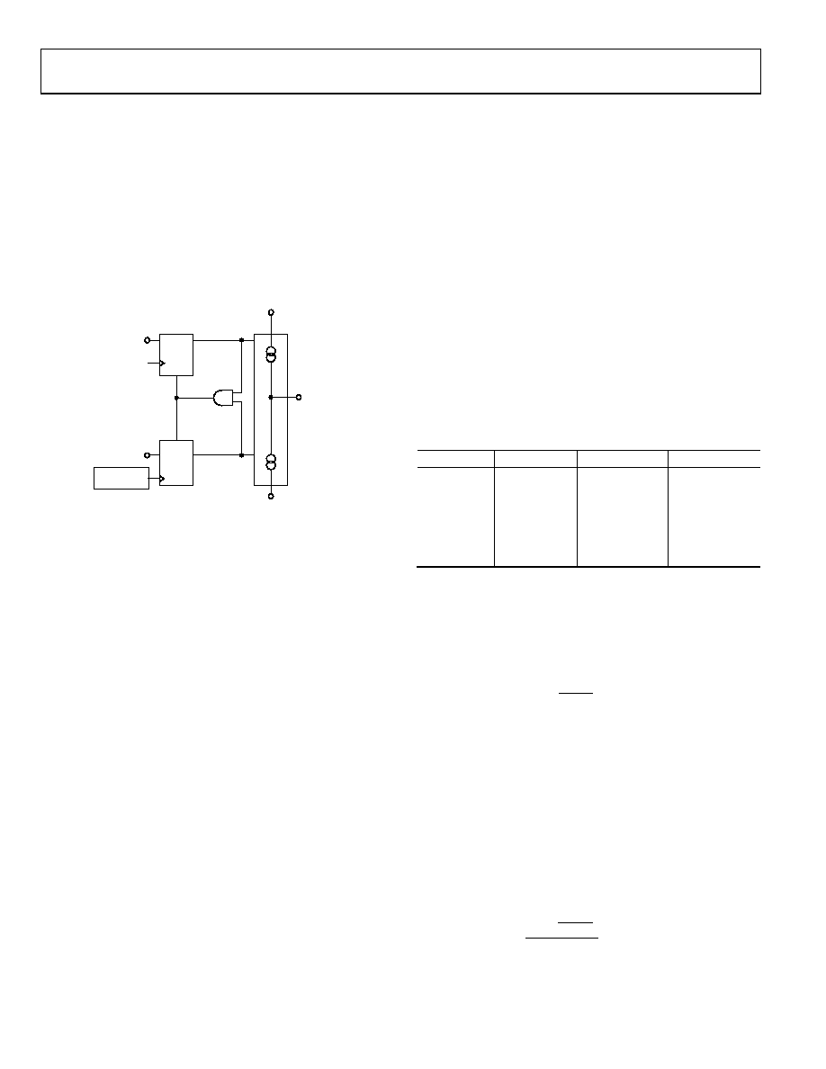
PLL1 PHASE FREQUENCY DETECTOR (PFD) AND
CHARGE PUMP
The PFD determines the phase difference error between the
reference divider output and the feedback divider output clock
edges. The outputs of this circuit are pulse-width modulated up
and down signal pulses. These pulses drive the charge pump
circuit. The amount of charge delivered from the charge pump to
the loop filter is determined by the instantaneous phase error. The
action of the closed loop is to drive the frequency and phase error
at the input of the PFD toward zero. Figure 42 shows a block
diagram of the PFD/CP circuitry.
D1 Q1
CLR1
REFCLK
HIGH
UP
D2 Q2
CLR2
HIGH
DOWN
CP
CHARGE
PUMP
3.3V
GND
FEEDBACK
DIVIDER
09
284
-04
7
Figure 42. PFD Circuit Showing Simplified Charge Pump
PLL1 VCO
PLL1 incorporates a low phase noise LC-tank VCO. This VCO
has 32 frequency bands spanning from 2.15 GHz to 2.55 GHz.
At power-up, a VCO calibration cycle begins and the correct band
is selected based on the feedback divider setting (Na). Whenever a
new feedback divider setting is called for, the VCO calibration
process must run by writing 1 followed by 0 to the NewAcq bit,
Register X0[0].
PLL1 FEEDBACK DIVIDER
The feedback divider ratio, Na, is used to set the PLL1 VCO
frequency according to Equation 3. Note that the Na value is set
by adding the offset value of 80 to the value programmed to
Register AF0[5:0], where 80 is the minimum divider Na value.
The maximum Na value is 131. For example, to set Na to 85, the
AF0[5:0] register is set to 5.
SETTING THE OUTPUT FREQUENCY OF PLL1
For example, set the output frequency (fOUT0) on Port 0 to
156.25 MHz, the output frequency (fOUT1) on Port 1 to 100 MHz,
and both the reference frequency (fREF) and the PFD frequency
(fPFD) to 25 MHz.
The frequency fOUT0 presented to OUT0 can be set according to
Equation 4.
The frequency fOUT1 presented to OUT1 can be set according to
Equation 5.
To determine if both 156.25 MHz and 100 MHz can be derived
from a common fVCO1 frequency in the 2.15 GHz to 2.55 GHz
range, use the lowest common multiple (LCM) of 156.25 MHz
and 100 MHz to determine the lowest VCO frequency that can
be divided down to provide both of these frequencies.
LCM(156.25 MHz, 100 MHz) = 2.5 GHz
(6)
Therefore, set the VCO frequency to 2.5 GHz. With fPFD =
25 MHz, from Equation 3, Na must be set to 100.
For 156.25 MHz on Port 0, set
V0 × D0 = 16
(7)
This can be achieved by setting V0 to 4 and D0 to 4. For
100 MHz on Port 1, set
V1 × D1 = 25
(8)
This can be achieved by setting V1 to 5 and D1 to 5. With a
reference frequency of 25 MHz, the reference divider value, R,
must be set to 1 by setting Register G0[1] to 0. Table 22
summarizes the register settings for this configuration.
Table 22. Register Settings for Example PLL1 Configuration
Parameter
Divide Value
I2C Register
Register Value
Na
100
AF0[5:0]
010100
V0
4
ADV0[7:5]
100
D0
4
ADV0[4:0]
00100
V1
5
ADV1[7:5]
101
D1
5
ADV1[4:0]
00101
R
1
G0[1]
1
PLL2 INTEGER/FRACTIONAL-N PLL
The lower PLL in Figure 32, PLL2, is a fractional-N PLL. The
input frequency to the PLL from the reference circuit is fPFD.
The VCO frequency, fVCO2, is programmed by setting the values
for Nb, FRAC, and MOD according to
)
(
2
MOD
FRAC
Nb
f
PFD
VCO
+
×
=
(9)
where Nb is programmable in the 80 to 131 range. To provide
the greatest flexibility and accuracy, both the FRAC and MOD
values can be programmed to a resolution of 12 bits, where
FRAC < MOD. The VCO output frequency can tune over the
2.15 GHz to 2.55 GHz range to fractional multiples of the PFD
input frequency.
By setting each of the VCO divider (V2 and V3) and output
divider (D2 and D3) values, the VCO frequency can be divided
down to the required output frequency, independently, for each
of the output ports, OUT2 and OUT3. The fOUT2frequency
presented to OUT2 can be set according to
D2
V2
MOD
FRAC
Nb
f
PFD
OUT2
×
+
×
=
)
(
(10)
相关PDF资料 |
PDF描述 |
|---|---|
| D38999/24FG11PA | CONN RCPT 11POS JAM NUT W/PINS |
| VE-J5J-MW-B1 | CONVERTER MOD DC/DC 36V 100W |
| VE-J4D-MX-F4 | CONVERTER MOD DC/DC 85V 75W |
| LT8500IUHH#PBF | IC PWM GENERATOR 56-QFN |
| VE-J4F-MX-F3 | CONVERTER MOD DC/DC 72V 75W |
相关代理商/技术参数 |
参数描述 |
|---|---|
| AD9577-EVALZ | 制造商:AD 制造商全称:Analog Devices 功能描述:Clock Generator with Dual PLLs |
| AD9578BCPZ | 功能描述:IC PLL CLOCK GEN 20MHZ 48LFCSP 制造商:analog devices inc. 系列:- 包装:托盘 零件状态:有效 类型:* PLL:带旁路 输入:LVCMOS,LVDS,LVPECL,晶体 输出:HCSL,LVCMOS,LVDS,LVPECL 电路数:1 比率 - 输入:输出:2:5 差分 - 输入:输出:是/是 频率 - 最大值:919MHz 分频器/倍频器:是/无 电压 - 电源:2.375 V ~ 3.63 V 工作温度:-25°C ~ 85°C 安装类型:表面贴装 封装/外壳:48-WFQFN 裸露焊盘,CSP 供应商器件封装:48-LFCSP-VQ(7x7) 标准包装:1 |
| AD9578BCPZ-REEL7 | 功能描述:IC PLL CLOCK GEN 20MHZ 48LFCSP 制造商:analog devices inc. 系列:- 包装:剪切带(CT) 零件状态:有效 类型:* PLL:带旁路 输入:LVCMOS,LVDS,LVPECL,晶体 输出:HCSL,LVCMOS,LVDS,LVPECL 电路数:1 比率 - 输入:输出:2:5 差分 - 输入:输出:是/是 频率 - 最大值:919MHz 分频器/倍频器:是/无 电压 - 电源:2.375 V ~ 3.63 V 工作温度:-25°C ~ 85°C 安装类型:表面贴装 封装/外壳:48-WFQFN 裸露焊盘,CSP 供应商器件封装:48-LFCSP-VQ(7x7) 标准包装:1 |
| AD95S08KAC | 制造商:未知厂家 制造商全称:未知厂家 功能描述:THYRISTOR MODULE|DOUBLER|HALF-CNTLD|POSITIVE|15V V(RRM)|95A I(T) |
| AD95S08KAF | 制造商:未知厂家 制造商全称:未知厂家 功能描述:THYRISTOR MODULE|DOUBLER|HALF-CNTLD|POSITIVE|15V V(RRM)|95A I(T) |
发布紧急采购,3分钟左右您将得到回复。