- 您现在的位置:买卖IC网 > PDF目录16806 > ADM1166ACPZ (Analog Devices Inc)IC SEQUENCER/SUPERVISOR 40LFCSP PDF资料下载
参数资料
| 型号: | ADM1166ACPZ |
| 厂商: | Analog Devices Inc |
| 文件页数: | 1/32页 |
| 文件大小: | 0K |
| 描述: | IC SEQUENCER/SUPERVISOR 40LFCSP |
| 标准包装: | 1 |
| 系列: | Super Sequencer® |
| 应用: | 电源监控器,序列发生器 |
| 输入电压: | 3 V ~ 14.4 V |
| 电源电压: | 3 V ~ 14.4 V |
| 电流 - 电源: | 4.2mA |
| 工作温度: | -40°C ~ 85°C |
| 安装类型: | 表面贴装 |
| 封装/外壳: | 40-WFQFN 裸露焊盘,CSP |
| 供应商设备封装: | 40-LFCSP-WQ(6x6) |
| 包装: | 托盘 |
当前第1页第2页第3页第4页第5页第6页第7页第8页第9页第10页第11页第12页第13页第14页第15页第16页第17页第18页第19页第20页第21页第22页第23页第24页第25页第26页第27页第28页第29页第30页第31页第32页
�� �����
�����
�����Super� Sequencer� with� Margining� Control�
�and� Nonvolatile� Fault� Recording�
�ADM1166�
�FEATURES�
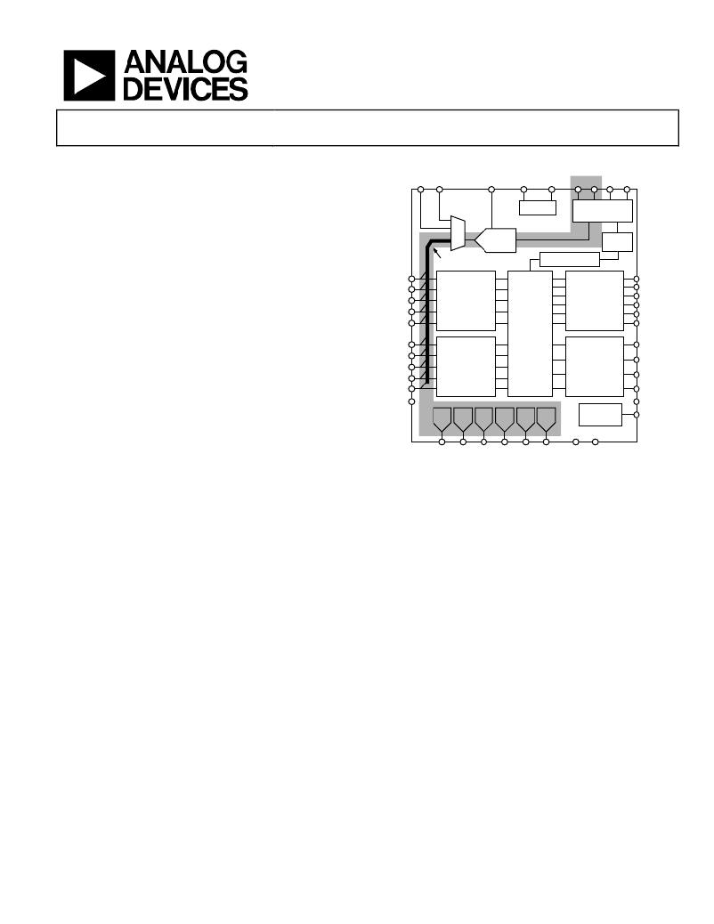
�FUNCTIONAL� BLOCK� DIAGRAM�
�Complete� supervisory� and� sequencing� solution� for� up� to�
�10� supplies�
�16� event� deep� black� box� nonvolatile� fault� recording�
�AUX1� AUX2�
�REFIN�
�ADM1166�
�REFOUT� REFGND�
�VREF�
�SDA� SCL� A1�
�SMBus�
�INTERFACE�
�A0�
�10� supply� fault� detectors� enable� supervision� of� supplies� to�
�<0.5%� accuracy� at� all� voltages� at� 25°C�
�<1.0%� accuracy� across� all� voltages� and� temperatures�
�5� selectable� input� attenuators� allow� supervision� of� supplies� to�
�12-BIT�
�SAR� ADC�
�CLOSED-LOOP�
�MARGINING� SYSTEM�
�FAULT� RECORDING�
�EEPROM�
�14.4� V� on� VH�
�6� V� on� VP1� to� VP4� (VPx)�
�5� dual-function� inputs,� VX1� to� VX5� (VXx)�
�High� impedance� input� to� supply� fault� detector� with�
�thresholds� between� 0.573� V� and� 1.375� V�
�General-purpose� logic� input�
�10� programmable� driver� outputs,� PDO1� to� PDO10� (PDOx)�
�Open-collector� with� external� pull-up�
�VX1�
�VX2�
�VX3�
�VX4�
�VX5�
�VP1�
�VP2�
�VP3�
�VP4�
�DUAL-�
�FUNCTION�
�INPUTS�
�(LOGIC� INPUTS�
�OR�
�SFDs)�
�PROGRAMMABLE�
�RESET�
�GENERATORS�
�(SFDs)�
�SEQUENCING�
�ENGINE�
�CONFIGURABLE�
�OUTPUT�
�DRIVERS�
�(HV� CAPABLE� OF�
�DRIVING� GATES�
�OF� N-FET)�
�CONFIGURABLE�
�OUTPUT�
�DRIVERS�
�(LV� CAPABLE�
�OF� DRIVING�
�LOGIC� SIGNALS)�
�PDO1�
�PDO2�
�PDO3�
�PDO4�
�PDO5�
�PDO6�
�PDO7�
�PDO8�
�PDO9�
�Push/pull� output,� driven� to� VDDCAP� or� VPx�
�VH�
�PDO10�
�Open� collector� with� weak� pull-up� to� VDDCAP� or� VPx�
�Internally� charge-pumped� high� drive� for� use� with� external�
�AGND�
�V� OUT�
�DAC�
�V� OUT�
�DAC�
�V� OUT�
�DAC�
�V� OUT�
�DAC�
�V� OUT�
�DAC�
�V� OUT�
�DAC�
�VDD�
�ARBITRATOR�
�PDOGND�
�VDDCAP�
�N-FET� (PDO1� to� PDO6� only)�
�Sequencing� engine� (SE)� implements� state� machine� control� of�
�DAC1� DAC2� DAC3� DAC4� DAC5� DAC6�
�VCCP� GND�
�PDO� outputs�
�State� changes� conditional� on� input� events�
�Enables� complex� control� of� boards�
�Power-up� and� power-down� sequence� control�
�Fault� event� handling�
�Interrupt� generation� on� warnings�
�Watchdog� function� can� be� integrated� in� SE�
�Program� software� control� of� sequencing� through� SMBus�
�Complete� voltage-margining� solution� for� 6� voltage� rails�
�6� voltage� output� 8-bit� DACs� (0.300� V� to� 1.551� V)� allow� voltage�
�adjustment� via� dc-to-dc� converter� trim/feedback� node�
�12-bit� ADC� for� readback� of� all� supervised� voltages�
�2� auxiliary� (single-ended)� ADC� inputs�
�Reference� input� (REFIN)� has� 2� input� options�
�Driven� directly� from� 2.048� V� (±0.25%)� REFOUT� pin�
�More� accurate� external� reference� for� improved� ADC�
�performance�
�Device� powered� by� the� highest� of� VPx,� VH� for� improved�
�redundancy�
�User� EEPROM:� 256� bytes�
�Industry-standard� 2-wire� bus� interface� (SMBus)�
�Guaranteed� PDO� low� with� VH,� VPx� =� 1.2� V�
�Available� in� 40-lead,� 6� mm� � 6� mm� LFCSP� and�
�48-lead,� 7� mm� � 7� mm� TQFP� packages�
�For� more� information� about� the� ADM1166� register� map,�
�refer� to� the� AN-698� Application� Note�
�Rev.� 0�
�Information� furnished� by� Analog� Devices� is� believed� to� be� accurate� and� reliable.� However,� no�
�responsibility� is� assumed� by� Analog� Devices� for� its� use,� nor� for� any� infringements� of� patents� or� other�
�rights� of� third� parties� that� may� result� from� its� use.� Specifications� subject� to� change� without� notice.� No�
�license� is� granted� by� implication� or� otherwise� under� any� patent� or� patent� rights� of� Analog� Devices.�
�Trademarks� and� registered� trademarks� are� the� property� of� their� respective� owners.�
�Figure� 1.�
�APPLICATIONS�
�Central� office� systems�
�Servers/routers�
�Multivoltage� system� line� cards�
�DSP/FPGA� supply� sequencing�
�In-circuit� testing� of� margined� supplies�
�GENERAL� DESCRIPTION�
�The� ADM1166� Super� Sequencer?� is� a� configurable� supervisory/�
�sequencing� device� that� offers� a� single-chip� solution� for� supply�
�monitoring� and� sequencing� in� multiple-supply� systems.� In� addition�
�to� these� functions,� the� ADM1166� integrates� a� 12-bit� ADC� and�
�six� 8-bit� voltage� output� DACs.� These� circuits� can� be� used� to�
�implement� a� closed-loop� margining� system� that� enables� supply�
�adjustment� by� altering� either� the� feedback� node� or� reference� of�
�a� dc-to-dc� converter� using� the� DAC� outputs.�
�Supply� margining� can� be� performed� with� a� minimum� of� external�
�components.� The� margining� loop� can� be� used� for� in-circuit� testing�
�of� a� board� during� production� (for� example,� to� verify� board� func-�
�tionality� at� ?5%� of� nominal� supplies),� or� it� can� be� used� dynamically�
�to� accurately� control� the� output� voltage� of� a� dc-to-dc� converter.�
�One� Technology� Way,� P.O.� Box� 9106,� Norwood,� MA� 02062-9106,� U.S.A.�
�Tel:� 781.329.4700� www.analog.com�
�Fax:� 781.461.3113� ?2010� Analog� Devices,� Inc.� All� rights� reserved.�
�相关PDF资料 |
PDF描述 |
|---|---|
| 0982661057 | CBL 35POS 0.5MM JMPR TYPE A 3" |
| H3AAS-1406G | IDC CABLE - HSC14S/AE14G/HSC14S |
| V300B3V3E100B2 | CONVERTER MOD DC/DC 3.3V 100W |
| H2MXS-1406M | DIP CABLE - HDM14S/AE14M/X |
| GCM12DRYN-S13 | CONN EDGECARD 24POS .156 EXTEND |
相关代理商/技术参数 |
参数描述 |
|---|---|
| ADM1166ACPZ-REEL | 功能描述:IC SEQUENCER/SUPERVISOR 40LFCSP RoHS:是 类别:集成电路 (IC) >> PMIC - 电源控制器,监视器 系列:Super Sequencer® 产品培训模块:Lead (SnPb) Finish for COTS Obsolescence Mitigation Program 标准包装:2,500 系列:- 应用:多相控制器 输入电压:- 电源电压:9 V ~ 14 V 电流 - 电源:- 工作温度:-40°C ~ 85°C 安装类型:表面贴装 封装/外壳:40-WFQFN 裸露焊盘 供应商设备封装:40-TQFN-EP(5x5) 包装:带卷 (TR) |
| ADM1166ARTZ | 制造商:Analog Devices 功能描述:SUPER SEQUENCER W/ BLACK BOX - Tape and Reel |
| ADM1166ASUZ | 功能描述:IC SEQUENCER/SUPERVISOR 48TQFP RoHS:是 类别:集成电路 (IC) >> PMIC - 电源控制器,监视器 系列:Super Sequencer® 产品培训模块:Lead (SnPb) Finish for COTS Obsolescence Mitigation Program 标准包装:2,500 系列:- 应用:多相控制器 输入电压:- 电源电压:9 V ~ 14 V 电流 - 电源:- 工作温度:-40°C ~ 85°C 安装类型:表面贴装 封装/外壳:40-WFQFN 裸露焊盘 供应商设备封装:40-TQFN-EP(5x5) 包装:带卷 (TR) |
| ADM1166ASUZ-REEL | 功能描述:IC SEQUENCER/SUPERVISOR 48TQFP RoHS:是 类别:集成电路 (IC) >> PMIC - 电源控制器,监视器 系列:Super Sequencer® 产品培训模块:Lead (SnPb) Finish for COTS Obsolescence Mitigation Program 标准包装:2,500 系列:- 应用:多相控制器 输入电压:- 电源电压:9 V ~ 14 V 电流 - 电源:- 工作温度:-40°C ~ 85°C 安装类型:表面贴装 封装/外壳:40-WFQFN 裸露焊盘 供应商设备封装:40-TQFN-EP(5x5) 包装:带卷 (TR) |
| ADM1166ASUZ-REEL7 | 功能描述:IC SEQUENCER/SUPERVISOR 48TQFP RoHS:是 类别:集成电路 (IC) >> PMIC - 电源控制器,监视器 系列:Super Sequencer® 产品培训模块:Lead (SnPb) Finish for COTS Obsolescence Mitigation Program 标准包装:2,500 系列:- 应用:多相控制器 输入电压:- 电源电压:9 V ~ 14 V 电流 - 电源:- 工作温度:-40°C ~ 85°C 安装类型:表面贴装 封装/外壳:40-WFQFN 裸露焊盘 供应商设备封装:40-TQFN-EP(5x5) 包装:带卷 (TR) |
发布紧急采购,3分钟左右您将得到回复。