- 您现在的位置:买卖IC网 > PDF目录16806 > ADM1166ACPZ (Analog Devices Inc)IC SEQUENCER/SUPERVISOR 40LFCSP PDF资料下载
参数资料
| 型号: | ADM1166ACPZ |
| 厂商: | Analog Devices Inc |
| 文件页数: | 25/32页 |
| 文件大小: | 0K |
| 描述: | IC SEQUENCER/SUPERVISOR 40LFCSP |
| 标准包装: | 1 |
| 系列: | Super Sequencer® |
| 应用: | 电源监控器,序列发生器 |
| 输入电压: | 3 V ~ 14.4 V |
| 电源电压: | 3 V ~ 14.4 V |
| 电流 - 电源: | 4.2mA |
| 工作温度: | -40°C ~ 85°C |
| 安装类型: | 表面贴装 |
| 封装/外壳: | 40-WFQFN 裸露焊盘,CSP |
| 供应商设备封装: | 40-LFCSP-WQ(6x6) |
| 包装: | 托盘 |
第1页第2页第3页第4页第5页第6页第7页第8页第9页第10页第11页第12页第13页第14页第15页第16页第17页第18页第19页第20页第21页第22页第23页第24页当前第25页第26页第27页第28页第29页第30页第31页第32页
�� ��
��
��ADM1166�
�COMMUNICATING� WITH� THE� ADM1166�
�CONFIGURATION� DOWNLOAD� AT� POWER-UP�
�The� configuration� of� the� ADM1166� (undervoltage/overvoltage�
�thresholds,� glitch� filter� timeouts,� and� PDO� configurations)� is�
�dictated� by� the� contents� of� the� RAM.� The� RAM� comprises� digital�
�latches� that� are� local� to� each� function� on� the� device.� The� latches� are�
�double� buffered� and� have� two� identical� latches,� Latch� A� and� Latch� B.�
�Therefore,� when� an� update� to� a� function� occurs,� the� contents� of�
�Latch� A� are� updated� first,� and� then� the� contents� of� Latch� B� are�
�updated� with� identical� data.� The� advantages� of� this� architecture� are�
�explained� in� detail� in� the� Updating� the� Configuration� section.�
�The� two� latches� are� volatile� memory� and� lose� their� contents� at�
�power-down.� Therefore,� the� configuration� in� the� RAM� must� be�
�restored� at� power-up� by� downloading� the� contents� of� the� EEPROM�
�(nonvolatile� memory)� to� the� local� latches.� This� download� occurs� in�
�steps,� as� follows:�
�1.� With� no� power� applied� to� the� device,� the� PDOs� are� all� high�
�impedance.�
�2.� When� 1.2� V� appears� on� any� of� the� inputs� connected� to� the�
�VDD� arbitrator� (VH� or� VPx),� the� PDOs� are� all� weakly�
�pulled� to� GND� with� a� 20� k� resistor.�
�3.� When� the� supply� rises� above� the� undervoltage� lockout� of�
�the� device� (UVLO� is� 2.5� V),� the� EEPROM� starts� to�
�download� to� the� RAM.�
�4.� The� EEPROM� downloads� its� contents� to� all� Latch� As.�
�5.� When� the� contents� of� the� EEPROM� are� completely�
�downloaded� to� the� Latch� As,� the� device� controller� signals�
�all� Latch� As� to� download� to� all� Latch� Bs� simultaneously,�
�completing� the� configuration� download.�
�6.� At� 0.5� ms� after� the� configuration� download� completes,� the� first�
�state� definition� is� downloaded� from� the� EEPROM� into� the� SE.�
�Note� that� any� attempt� to� communicate� with� the� device� prior� to�
�the� completion� of� the� download� causes� the� ADM1166� to� issue�
�a� no� acknowledge� (NACK).�
�UPDATING� THE� CONFIGURATION�
�After� power-up,� with� all� the� configuration� settings� loaded� from�
�the� EEPROM� into� the� RAM� registers,� the� user� may� need� to� alter�
�the� configuration� of� functions� on� the� ADM1166,� such� as� changing�
�the� undervoltage� or� overvoltage� limit� of� an� SFD,� changing� the� fault�
�output� of� an� SFD,� or� adjusting� the� rise� time� delay� of� one� of� the� PDOs.�
�The� ADM1166� provides� several� options� that� allow� the� user� to�
�update� the� configuration� over� the� SMBus� interface.� The� following�
�three� options� are� controlled� in� the� UPDCFG� register.�
�SMBus�
�Option� 1�
�Update� the� configuration� in� real� time.� The� user� writes� to� the� RAM�
�across� the� SMBus,� and� the� configuration� is� updated� immediately.�
�Option� 2�
�Update� the� Latch� As� without� updating� the� Latch� Bs.� With� this�
�method,� the� configuration� of� the� ADM1166� remains� unchanged�
�and� continues� to� operate� in� the� original� setup� until� the� instruction�
�is� given� to� update� the� Latch� Bs.�
�Option� 3�
�Change� the� EEPROM� register� contents� without� changing� the� RAM�
�contents,� and� then� download� the� revised� EEPROM� contents� to�
�the� RAM� registers.� With� this� method,� the� configuration� of� the�
�ADM1166� remains� unchanged� and� continues� to� operate� in� the�
�original� setup� until� the� instruction� is� given� to� update� the� RAM.�
�The� instruction� to� download� from� the� EEPROM� in� Option� 3� is�
�also� a� useful� way� to� restore� the� original� EEPROM� contents� if�
�revisions� to� the� configuration� are� unsatisfactory.� For� example,� if�
�the� user� needs� to� alter� an� overvoltage� threshold,� the� RAM� register�
�can� be� updated� as� described� in� the� Option� 1� section.� However,�
�if� the� user� is� not� satisfied� with� the� change� and� wants� to� revert� to�
�the� original� programmed� value,� the� device� controller� can� issue� a�
�command� to� download� the� EEPROM� contents� to� the� RAM� again,�
�as� described� in� the� Option� 3� section,� restoring� the� ADM1166� to�
�its� original� configuration.�
�The� topology� of� the� ADM1166� makes� this� type� of� operation�
�possible.� The� local,� volatile� registers� (RAM)� are� all� double-�
�buffered� latches.� Setting� Bit� 0� of� the� UPDCFG� register� to� 1� leaves�
�the� double-buffered� latches� open� at� all� times.� If� Bit� 0� is� set� to� 0�
�when� a� RAM� write� occurs� across� the� SMBus,� only� the� first� side�
�of� the� double-buffered� latch� is� written� to.� The� user� must� then�
�write� a� 1� to� Bit� 1� of� the� UPDCFG� register.� This� generates� a� pulse�
�to� update� all� the� second� latches� at� once.� EEPROM� writes� occur�
�in� a� similar� way.�
�The� final� bit� in� this� register� can� enable� or� disable� EEPROM� page�
�erasure.� If� this� bit� is� set� high,� the� contents� of� an� EEPROM� page� can�
�all� be� set� to� 1.� If� this� bit� is� set� low,� the� contents� of� a� page� cannot� be�
�erased,� even� if� the� command� code� for� page� erasure� is� programmed�
�across� the� SMBus.� The� bit� map� for� the� UPDCFG� register� is� shown�
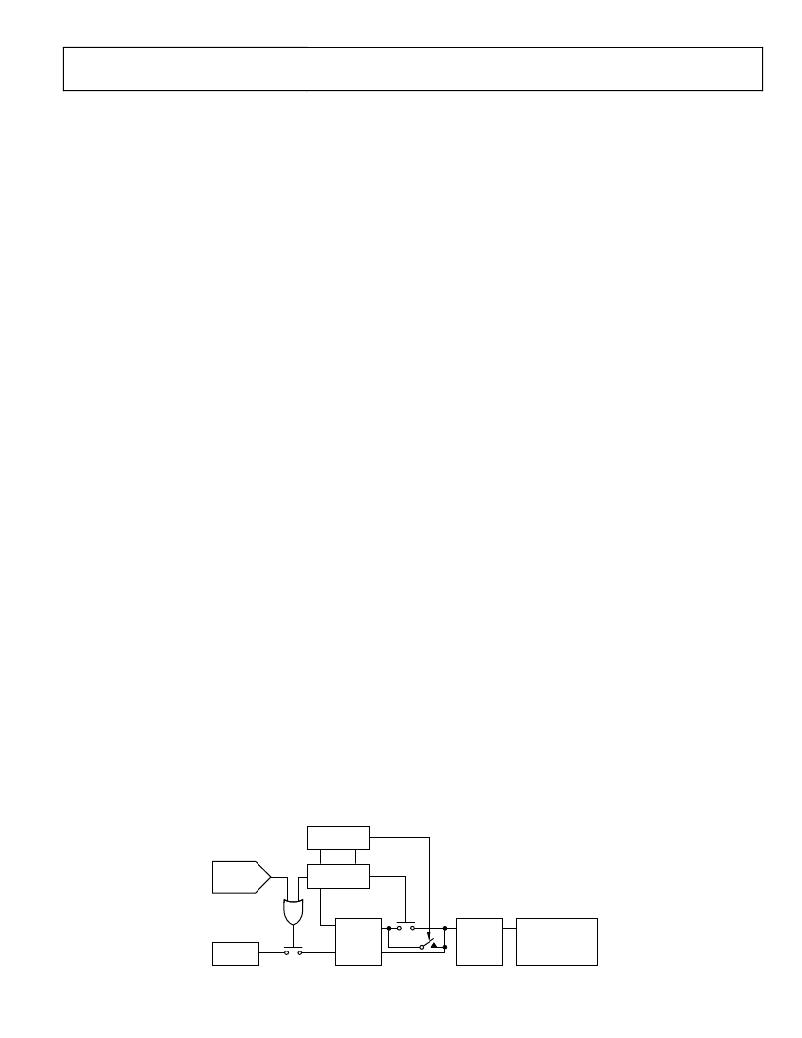
�in� the� AN-698� Application� Note.� A� flow� diagram� for� download� at�
�power-up� and� subsequent� configuration� updates� is� shown� in�
��POWER-UP�
�DEVICE�
�(V� CC� >� 2.5V)�
�E�
�CONTROLLER�
�R�
�U�
�E�
�P�
�R�
�O�
�M�
�L�
�D�
�D�
�A�
�T�
�A�
�LATCH� A�
�A�
�M�
�L�
�D�
�P�
�D�
�LATCH� B�
�FUNCTION�
�(OV� THRESHOLD�
�EEPROM�
�Figure� 35.� Configuration� Update� Flow� Diagram�
�Rev.� 0� |� Page� 25� of� 32�
�ON� VP1)�
�相关PDF资料 |
PDF描述 |
|---|---|
| 0982661057 | CBL 35POS 0.5MM JMPR TYPE A 3" |
| H3AAS-1406G | IDC CABLE - HSC14S/AE14G/HSC14S |
| V300B3V3E100B2 | CONVERTER MOD DC/DC 3.3V 100W |
| H2MXS-1406M | DIP CABLE - HDM14S/AE14M/X |
| GCM12DRYN-S13 | CONN EDGECARD 24POS .156 EXTEND |
相关代理商/技术参数 |
参数描述 |
|---|---|
| ADM1166ACPZ-REEL | 功能描述:IC SEQUENCER/SUPERVISOR 40LFCSP RoHS:是 类别:集成电路 (IC) >> PMIC - 电源控制器,监视器 系列:Super Sequencer® 产品培训模块:Lead (SnPb) Finish for COTS Obsolescence Mitigation Program 标准包装:2,500 系列:- 应用:多相控制器 输入电压:- 电源电压:9 V ~ 14 V 电流 - 电源:- 工作温度:-40°C ~ 85°C 安装类型:表面贴装 封装/外壳:40-WFQFN 裸露焊盘 供应商设备封装:40-TQFN-EP(5x5) 包装:带卷 (TR) |
| ADM1166ARTZ | 制造商:Analog Devices 功能描述:SUPER SEQUENCER W/ BLACK BOX - Tape and Reel |
| ADM1166ASUZ | 功能描述:IC SEQUENCER/SUPERVISOR 48TQFP RoHS:是 类别:集成电路 (IC) >> PMIC - 电源控制器,监视器 系列:Super Sequencer® 产品培训模块:Lead (SnPb) Finish for COTS Obsolescence Mitigation Program 标准包装:2,500 系列:- 应用:多相控制器 输入电压:- 电源电压:9 V ~ 14 V 电流 - 电源:- 工作温度:-40°C ~ 85°C 安装类型:表面贴装 封装/外壳:40-WFQFN 裸露焊盘 供应商设备封装:40-TQFN-EP(5x5) 包装:带卷 (TR) |
| ADM1166ASUZ-REEL | 功能描述:IC SEQUENCER/SUPERVISOR 48TQFP RoHS:是 类别:集成电路 (IC) >> PMIC - 电源控制器,监视器 系列:Super Sequencer® 产品培训模块:Lead (SnPb) Finish for COTS Obsolescence Mitigation Program 标准包装:2,500 系列:- 应用:多相控制器 输入电压:- 电源电压:9 V ~ 14 V 电流 - 电源:- 工作温度:-40°C ~ 85°C 安装类型:表面贴装 封装/外壳:40-WFQFN 裸露焊盘 供应商设备封装:40-TQFN-EP(5x5) 包装:带卷 (TR) |
| ADM1166ASUZ-REEL7 | 功能描述:IC SEQUENCER/SUPERVISOR 48TQFP RoHS:是 类别:集成电路 (IC) >> PMIC - 电源控制器,监视器 系列:Super Sequencer® 产品培训模块:Lead (SnPb) Finish for COTS Obsolescence Mitigation Program 标准包装:2,500 系列:- 应用:多相控制器 输入电压:- 电源电压:9 V ~ 14 V 电流 - 电源:- 工作温度:-40°C ~ 85°C 安装类型:表面贴装 封装/外壳:40-WFQFN 裸露焊盘 供应商设备封装:40-TQFN-EP(5x5) 包装:带卷 (TR) |
发布紧急采购,3分钟左右您将得到回复。