- 您现在的位置:买卖IC网 > PDF目录16806 > ADM1166ACPZ (Analog Devices Inc)IC SEQUENCER/SUPERVISOR 40LFCSP PDF资料下载
参数资料
| 型号: | ADM1166ACPZ |
| 厂商: | Analog Devices Inc |
| 文件页数: | 29/32页 |
| 文件大小: | 0K |
| 描述: | IC SEQUENCER/SUPERVISOR 40LFCSP |
| 标准包装: | 1 |
| 系列: | Super Sequencer® |
| 应用: | 电源监控器,序列发生器 |
| 输入电压: | 3 V ~ 14.4 V |
| 电源电压: | 3 V ~ 14.4 V |
| 电流 - 电源: | 4.2mA |
| 工作温度: | -40°C ~ 85°C |
| 安装类型: | 表面贴装 |
| 封装/外壳: | 40-WFQFN 裸露焊盘,CSP |
| 供应商设备封装: | 40-LFCSP-WQ(6x6) |
| 包装: | 托盘 |
第1页第2页第3页第4页第5页第6页第7页第8页第9页第10页第11页第12页第13页第14页第15页第16页第17页第18页第19页第20页第21页第22页第23页第24页第25页第26页第27页第28页当前第29页第30页第31页第32页
�� �
�
�ADM1166�
�WRITE� OPERATIONS�
�The� SMBus� specification� defines� several� protocols� for� different�
�types� of� read� and� write� operations.� The� following� abbreviations�
��?� S� =� Start�
�?� P� =� Stop�
�?� R� =� Read�
�The� master� sends� a� command� code� telling� the� slave� device�
�to� erase� the� page.� The� ADM1166� command� code� for� a� page�
�erasure� is� 0xFE� (1111� 1110).� Note� that� for� a� page� erasure� to�
�take� place,� the� page� address� must� be� given� in� the� previous�
�write� word� transaction� (see� the� Write� Byte/Word� section).� In�
�addition,� Bit� 2� in� the� UPDCFG� register� (Address� 0x90)�
�must� be� set� to� 1.�
�1� 2� 3� 4� 5� 6�
�?�
�?�
�W� =� Write�
�A� =� Acknowledge�
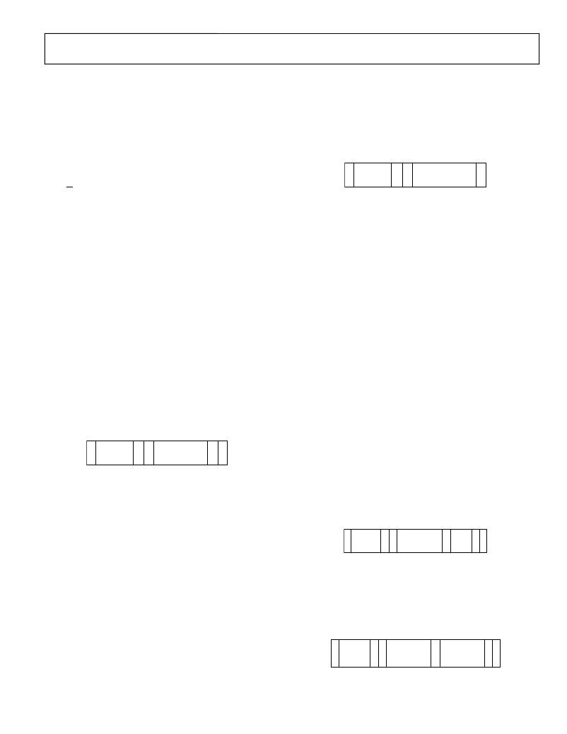
�S�
�SLAVE�
�ADDRESS�
�W�
�A�
�COMMAND�
�BYTE�
�(0xFE)�
�A�
�P�
�?�
�A� =� No� acknowledge�
�Figure� 40.� EEPROM� Page� Erasure�
�The� ADM1166� uses� the� following� SMBus� write� protocols.�
�Send� Byte�
�In� a� send� byte� operation,� the� master� device� sends� a� single�
�command� byte� to� a� slave� device,� as� follows:�
�As� soon� as� the� ADM1166� receives� the� command� byte,�
�page� erasure� begins.� The� master� device� can� send� a� stop�
�command� as� soon� as� it� sends� the� command� byte.� Page�
�erasure� takes� approximately� 20� ms.� If� the� ADM1166� is�
�accessed� before� erasure� is� complete,� it� responds� with� a�
�1.�
�2.�
�3.�
�The� master� device� asserts� a� start� condition� on� SDA.�
�The� master� sends� the� 7-bit� slave� address� followed� by� the�
�write� bit� (low).�
�The� addressed� slave� device� asserts� an� acknowledge� (ACK)�
�on� SDA.�
�no� acknowledge� (NACK).�
�Write� Byte/Word�
�In� a� write� byte/word� operation,� the� master� device� sends� a� command�
�byte� and� one� or� two� data� bytes� to� the� slave� device,� as� follows:�
�4.�
�5.�
�6.�
�The� master� sends� a� command� code.�
�The� slave� asserts� an� ACK� on� SDA.�
�The� master� asserts� a� stop� condition� on� SDA,� and� the�
�1.�
�2.�
�The� master� device� asserts� a� start� condition� on� SDA.�
�The� master� sends� the� 7-bit� slave� address� followed� by� the�
�write� bit� (low).�
�transaction� ends.�
�In� the� ADM1166,� the� send� byte� protocol� is� used� for� two�
�purposes:�
�?� To� write� a� register� address� to� the� RAM� for� a� subsequent�
�single� byte� read� from� the� same� address,� or� for� a� block� read�
��3.�
�4.�
�5.�
�6.�
�7.�
�8.�
�9.�
�The� addressed� slave� device� asserts� an� ACK� on� SDA.�
�The� master� sends� a� command� code.�
�The� slave� asserts� an� ACK� on� SDA.�
�The� master� sends� a� data� byte.�
�The� slave� asserts� an� ACK� on� SDA.�
�The� master� sends� a� data� byte� or� asserts� a� stop� condition.�
�The� slave� asserts� an� ACK� on� SDA.�
�1�
�2�
�3�
�4�
�5�
�6�
�10.� The� master� asserts� a� stop� condition� on� SDA� to� end� the�
�S�
�SLAVE�
�ADDRESS�
�W�
�A�
�RAM�
�ADDRESS�
�(0x00� TO� 0xDF)�
�A�
�P�
�transaction.�
�In� the� ADM1166,� the� write� byte/word� protocol� is� used� for� three�
�Figure� 39.� Setting� a� RAM� Address� for� Subsequent� Read�
�purposes:�
�?�
�To� erase� a� page� of� EEPROM� memory.� EEPROM� memory�
�can� be� written� to� only� if� it� is� unprogrammed.� Before� writing�
�to� one� or� more� EEPROM� memory� locations� that� are� already�
�?�
�To� write� a� single� byte� of� data� to� the� RAM.� In� this� case,� the�
�command� byte� is� RAM� Address� 0x00� to� RAM� Address� 0xDF,�
��programmed,� the� page(s)� containing� those� locations� must�
�1�
�2�
�3�
�4�
�5�
�6�
�7� 8�
�first� be� erased.� EEPROM� memory� is� erased� by� writing� a�
�command� byte.�
�S�
�SLAVE�
�ADDRESS�
�W� A�
�RAM�
�ADDRESS�
�(0x00� TO� 0xDF)�
�A� DATA� A� P�
�Figure� 41.� Single� Byte� Write� to� the� RAM�
�?�
�To� set� up� a� 2-byte� EEPROM� address� for� a� subsequent� read,�
�write,� block� read,� block� write,� or� page� erase.� In� this� case,� the�
�command� byte� is� the� high� byte� of� EEPROM� Address� 0xF8�
�to� EEPROM� Address� 0xFB.� The� only� data� byte� is� the� low�
��1�
�2�
�3�
�4�
�5�
�6�
�7� 8�
�EEPROM�
�EEPROM�
�S� W� A�
�SLAVE�
�ADDRESS�
�ADDRESS�
�HIGH� BYTE�
�A�
�ADDRESS�
�LOW� BYTE�
�A� P�
�(0xF8� TO� 0xFB)�
�(0x00� TO� 0xFF)�
�Figure� 42.� Setting� an� EEPROM� Address�
�Rev.� 0� |� Page� 29� of� 32�
�相关PDF资料 |
PDF描述 |
|---|---|
| 0982661057 | CBL 35POS 0.5MM JMPR TYPE A 3" |
| H3AAS-1406G | IDC CABLE - HSC14S/AE14G/HSC14S |
| V300B3V3E100B2 | CONVERTER MOD DC/DC 3.3V 100W |
| H2MXS-1406M | DIP CABLE - HDM14S/AE14M/X |
| GCM12DRYN-S13 | CONN EDGECARD 24POS .156 EXTEND |
相关代理商/技术参数 |
参数描述 |
|---|---|
| ADM1166ACPZ-REEL | 功能描述:IC SEQUENCER/SUPERVISOR 40LFCSP RoHS:是 类别:集成电路 (IC) >> PMIC - 电源控制器,监视器 系列:Super Sequencer® 产品培训模块:Lead (SnPb) Finish for COTS Obsolescence Mitigation Program 标准包装:2,500 系列:- 应用:多相控制器 输入电压:- 电源电压:9 V ~ 14 V 电流 - 电源:- 工作温度:-40°C ~ 85°C 安装类型:表面贴装 封装/外壳:40-WFQFN 裸露焊盘 供应商设备封装:40-TQFN-EP(5x5) 包装:带卷 (TR) |
| ADM1166ARTZ | 制造商:Analog Devices 功能描述:SUPER SEQUENCER W/ BLACK BOX - Tape and Reel |
| ADM1166ASUZ | 功能描述:IC SEQUENCER/SUPERVISOR 48TQFP RoHS:是 类别:集成电路 (IC) >> PMIC - 电源控制器,监视器 系列:Super Sequencer® 产品培训模块:Lead (SnPb) Finish for COTS Obsolescence Mitigation Program 标准包装:2,500 系列:- 应用:多相控制器 输入电压:- 电源电压:9 V ~ 14 V 电流 - 电源:- 工作温度:-40°C ~ 85°C 安装类型:表面贴装 封装/外壳:40-WFQFN 裸露焊盘 供应商设备封装:40-TQFN-EP(5x5) 包装:带卷 (TR) |
| ADM1166ASUZ-REEL | 功能描述:IC SEQUENCER/SUPERVISOR 48TQFP RoHS:是 类别:集成电路 (IC) >> PMIC - 电源控制器,监视器 系列:Super Sequencer® 产品培训模块:Lead (SnPb) Finish for COTS Obsolescence Mitigation Program 标准包装:2,500 系列:- 应用:多相控制器 输入电压:- 电源电压:9 V ~ 14 V 电流 - 电源:- 工作温度:-40°C ~ 85°C 安装类型:表面贴装 封装/外壳:40-WFQFN 裸露焊盘 供应商设备封装:40-TQFN-EP(5x5) 包装:带卷 (TR) |
| ADM1166ASUZ-REEL7 | 功能描述:IC SEQUENCER/SUPERVISOR 48TQFP RoHS:是 类别:集成电路 (IC) >> PMIC - 电源控制器,监视器 系列:Super Sequencer® 产品培训模块:Lead (SnPb) Finish for COTS Obsolescence Mitigation Program 标准包装:2,500 系列:- 应用:多相控制器 输入电压:- 电源电压:9 V ~ 14 V 电流 - 电源:- 工作温度:-40°C ~ 85°C 安装类型:表面贴装 封装/外壳:40-WFQFN 裸露焊盘 供应商设备封装:40-TQFN-EP(5x5) 包装:带卷 (TR) |
发布紧急采购,3分钟左右您将得到回复。