- 您现在的位置:买卖IC网 > PDF目录16806 > ADM1166ACPZ (Analog Devices Inc)IC SEQUENCER/SUPERVISOR 40LFCSP PDF资料下载
参数资料
| 型号: | ADM1166ACPZ |
| 厂商: | Analog Devices Inc |
| 文件页数: | 15/32页 |
| 文件大小: | 0K |
| 描述: | IC SEQUENCER/SUPERVISOR 40LFCSP |
| 标准包装: | 1 |
| 系列: | Super Sequencer® |
| 应用: | 电源监控器,序列发生器 |
| 输入电压: | 3 V ~ 14.4 V |
| 电源电压: | 3 V ~ 14.4 V |
| 电流 - 电源: | 4.2mA |
| 工作温度: | -40°C ~ 85°C |
| 安装类型: | 表面贴装 |
| 封装/外壳: | 40-WFQFN 裸露焊盘,CSP |
| 供应商设备封装: | 40-LFCSP-WQ(6x6) |
| 包装: | 托盘 |
第1页第2页第3页第4页第5页第6页第7页第8页第9页第10页第11页第12页第13页第14页当前第15页第16页第17页第18页第19页第20页第21页第22页第23页第24页第25页第26页第27页第28页第29页第30页第31页第32页
�� �
�
�ADM1166�
�The� hysteresis� value� is� given� by�
�V� HYST� =� V� R� � N� THRESH� /255�
�where:�
�V� HYST� is� the� desired� hysteresis� voltage.�
�N� THRESH� is� the� decimal� value� of� the� 5-bit� hysteresis� code.�
�Note� that� N� THRESH� has� a� maximum� value� of� 31.� The� maximum�
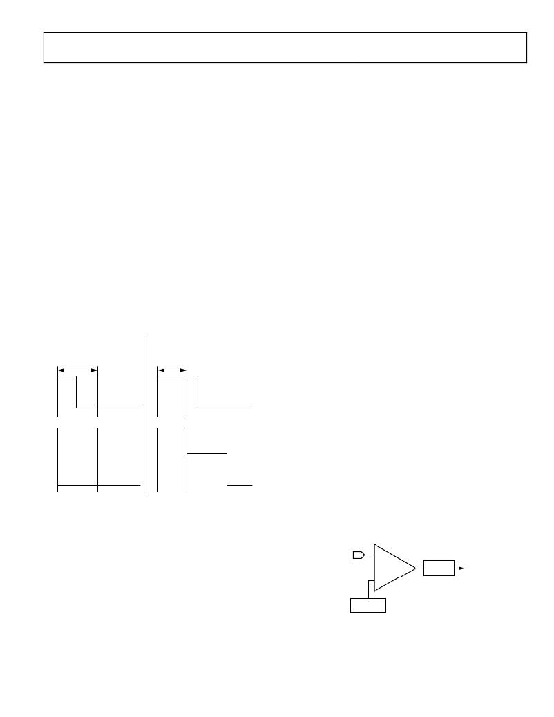
��INPUT� GLITCH� FILTERING�
�The� final� stage� of� the� SFDs� is� a� glitch� filter.� This� block� provides�
�time-domain� filtering� on� the� output� of� the� SFD� comparators,�
�which� allows� the� user� to� remove� any� spurious� transitions� such�
�as� supply� bounce� at� turn-on.� The� glitch� filter� function� is� in� addition�
�to� the� digitally� programmable� hysteresis� of� the� SFD� comparators.�
�The� glitch� filter� timeout� is� programmable� up� to� 100� μs.�
�For� example,� when� the� glitch� filter� timeout� is� 100� μs,� any� pulse�
�appearing� on� the� input� of� the� glitch� filter� block� that� is� less� than�
�100� μs� in� duration� is� prevented� from� appearing� on� the� output� of�
�the� glitch� filter� block.� Any� input� pulse� that� is� longer� than� 100� μs�
�appears� on� the� output� of� the� glitch� filter� block.� The� output� is�
�delayed� with� respect� to� the� input� by� 100� μs.� The� filtering� process� is�
��INPUT� PULSE� SHORTER� INPUT� PULSE� LONGER�
�THAN� GLITCH� FILTER� TIMEOUT� THAN� GLITCH� FILTER� TIMEOUT�
�An� additional� supply� supervision� function� is� available� when� the�
�VXx� pins� are� selected� as� digital� inputs.� In� this� case,� the� analog�
�function� is� available� as� a� second� detector� on� each� of� the� dedicated�
�analog� inputs,� VPx� and� VH.� The� analog� function� of� VX1� is�
�mapped� to� VP1,� VX2� is� mapped� to� VP2,� and� so� on.� VX5� is�
�mapped� to� VH.� In� this� case,� these� SFDs� can� be� viewed� as�
�secondary� or� warning� SFDs.�
�The� secondary� SFDs� are� fixed� to� the� same� input� range� as� the�
�primary� SFDs.� They� are� used� to� indicate� warning� levels� rather�
�than� failure� levels.� This� allows� faults� and� warnings� to� be� generated�
�on� a� single� supply� using� only� one� pin.� For� example,� if� VP1� is� set�
�to� output� a� fault� when� a� 3.3� V� supply� drops� to� 3.0� V,� VX1� can� be�
�set� to� output� a� warning� at� 3.1� V.� Warning� outputs� are� available� for�
�readback� from� the� status� registers.� They� are� also� OR’ed� together�
�and� fed� into� the� SE,� allowing� warnings� to� generate� interrupts� on�
�the� PDOs.� Therefore,� in� this� example,� if� the� supply� drops� to� 3.1� V,�
�a� warning� is� generated,� and� remedial� action� can� be� taken� before�
�the� supply� drops� out� of� tolerance.�
�VXx� PINS� AS� DIGITAL� INPUTS�
�As� discussed� in� the� Supply� Supervision� with� VXX� Inputs� section,�
�the� VXx� input� pins� on� the� ADM1166� have� dual� functionality.�
�The� second� function� is� as� a� digital� logic� input� to� the� device.�
�Therefore,� the� ADM1166� can� be� configured� for� up� to� five� digital�
�inputs.� These� inputs� are� TTL-/CMOS-compatible� inputs.� Standard�
�PROGRAMMED�
�TIMEOUT�
�INPUT�
�PROGRAMMED�
�TIMEOUT�
�INPUT�
�logic� signals� can� be� applied� to� the� pins:� RESET� from� reset� generators,�
�PWRGD� signals,� fault� flags,� and� manual� resets.� These� signals� are�
�available� as� inputs� to� the� SE� and,� therefore,� can� be� used� to� control�
�the� status� of� the� PDOs.� The� inputs� can� be� configured� to� detect�
�either� a� change� in� level� or� an� edge.�
�When� configured� for� level� detection,� the� output� of� the� digital�
�t� 0�
�t� GF�
�t� 0�
�t� GF�
�block� is� a� buffered� version� of� the� input.� When� configured� for� edge�
�detection,� a� pulse� of� programmable� width� is� output� from� the�
�digital� block� once� the� logic� transition� is� detected.� The� width� is�
�programmable� from� 0� μs� to� 100� μs.� The� digital� blocks� feature� the�
�same� glitch� filter� function� that� is� available� on� the� SFDs.� This�
�OUTPUT�
�OUTPUT�
�enables� the� user� to� ignore� spurious� transitions� on� the� inputs.� For�
�example,� the� filter� can� be� used� to� debounce� a� manual� reset� switch.�
�t� 0�
�t� GF�
�t� 0� t� GF�
�Figure� 23.� Input� Glitch� Filter� Function�
�When� configured� as� digital� inputs,� each� VXx� pin� has� a� weak�
�(10� μA)� pull-down� current� source� available� for� placing� the� input�
�SUPPLY� SUPERVISION� WITH� VXx� INPUTS�
�The� VXx� inputs� have� two� functions.� They� can� be� used� as� either�
�into� a� known� condition,� even� if� left� floating.� The� current� source,�
�if� selected,� weakly� pulls� the� input� to� GND.�
�supply� fault� detectors� or� digital� logic� inputs.� When� selected� as�
�analog� (SFD)� inputs,� the� VXx� pins� have� functionality� that� is� very�
�similar� to� the� VH� and� VPx� pins.� The� primary� difference� is� that� the�
�VXx�
�(DIGITAL� INPUT)�
�+�
�DETECTOR�
�GLITCH�
�FILTER�
�TO�
�SEQUENCING�
�ENGINE�
�VXx� pins� have� only� one� input� range:� 0.573� V� to� 1.375� V.� Therefore,�
�these� inputs� can� directly� supervise� only� the� very� low� supplies.�
�However,� the� input� impedance� of� the� VXx� pins� is� high,� allowing�
�an� external� resistor� divide� network� to� be� connected� to� the� pin.�
�Thus,� potentially� any� supply� can� be� divided� down� into� the� input�
�range� of� the� VXx� pin� and� supervised.� This� enables� the� ADM1166�
�to� monitor� other� supplies,� such� as� +24� V,� +48� V,� and� ?5� V.�
�Rev.� 0� |� Page� 15� of� 32�
�–�
�VREF� =� 1.4V�
�Figure� 24.� VXx� Digital� Input� Function�
�相关PDF资料 |
PDF描述 |
|---|---|
| 0982661057 | CBL 35POS 0.5MM JMPR TYPE A 3" |
| H3AAS-1406G | IDC CABLE - HSC14S/AE14G/HSC14S |
| V300B3V3E100B2 | CONVERTER MOD DC/DC 3.3V 100W |
| H2MXS-1406M | DIP CABLE - HDM14S/AE14M/X |
| GCM12DRYN-S13 | CONN EDGECARD 24POS .156 EXTEND |
相关代理商/技术参数 |
参数描述 |
|---|---|
| ADM1166ACPZ-REEL | 功能描述:IC SEQUENCER/SUPERVISOR 40LFCSP RoHS:是 类别:集成电路 (IC) >> PMIC - 电源控制器,监视器 系列:Super Sequencer® 产品培训模块:Lead (SnPb) Finish for COTS Obsolescence Mitigation Program 标准包装:2,500 系列:- 应用:多相控制器 输入电压:- 电源电压:9 V ~ 14 V 电流 - 电源:- 工作温度:-40°C ~ 85°C 安装类型:表面贴装 封装/外壳:40-WFQFN 裸露焊盘 供应商设备封装:40-TQFN-EP(5x5) 包装:带卷 (TR) |
| ADM1166ARTZ | 制造商:Analog Devices 功能描述:SUPER SEQUENCER W/ BLACK BOX - Tape and Reel |
| ADM1166ASUZ | 功能描述:IC SEQUENCER/SUPERVISOR 48TQFP RoHS:是 类别:集成电路 (IC) >> PMIC - 电源控制器,监视器 系列:Super Sequencer® 产品培训模块:Lead (SnPb) Finish for COTS Obsolescence Mitigation Program 标准包装:2,500 系列:- 应用:多相控制器 输入电压:- 电源电压:9 V ~ 14 V 电流 - 电源:- 工作温度:-40°C ~ 85°C 安装类型:表面贴装 封装/外壳:40-WFQFN 裸露焊盘 供应商设备封装:40-TQFN-EP(5x5) 包装:带卷 (TR) |
| ADM1166ASUZ-REEL | 功能描述:IC SEQUENCER/SUPERVISOR 48TQFP RoHS:是 类别:集成电路 (IC) >> PMIC - 电源控制器,监视器 系列:Super Sequencer® 产品培训模块:Lead (SnPb) Finish for COTS Obsolescence Mitigation Program 标准包装:2,500 系列:- 应用:多相控制器 输入电压:- 电源电压:9 V ~ 14 V 电流 - 电源:- 工作温度:-40°C ~ 85°C 安装类型:表面贴装 封装/外壳:40-WFQFN 裸露焊盘 供应商设备封装:40-TQFN-EP(5x5) 包装:带卷 (TR) |
| ADM1166ASUZ-REEL7 | 功能描述:IC SEQUENCER/SUPERVISOR 48TQFP RoHS:是 类别:集成电路 (IC) >> PMIC - 电源控制器,监视器 系列:Super Sequencer® 产品培训模块:Lead (SnPb) Finish for COTS Obsolescence Mitigation Program 标准包装:2,500 系列:- 应用:多相控制器 输入电压:- 电源电压:9 V ~ 14 V 电流 - 电源:- 工作温度:-40°C ~ 85°C 安装类型:表面贴装 封装/外壳:40-WFQFN 裸露焊盘 供应商设备封装:40-TQFN-EP(5x5) 包装:带卷 (TR) |
发布紧急采购,3分钟左右您将得到回复。