- 您现在的位置:买卖IC网 > PDF目录17412 > ADP1850DP-EVALZ (Analog Devices Inc)EVAL BOARD FOR ADP1850DP PDF资料下载
参数资料
| 型号: | ADP1850DP-EVALZ |
| 厂商: | Analog Devices Inc |
| 文件页数: | 14/32页 |
| 文件大小: | 0K |
| 描述: | EVAL BOARD FOR ADP1850DP |
| 标准包装: | 1 |
| 主要目的: | DC/DC,步降 |
| 输出及类型: | 1,非隔离 |
| 输出电压: | 1.09V |
| 电流 - 输出: | 50A |
| 输入电压: | 10 ~ 15 V |
| 稳压器拓扑结构: | 降压 |
| 频率 - 开关: | 300kHz |
| 板类型: | 完全填充 |
| 已供物品: | 板 |
| 已用 IC / 零件: | ADP1850DP |
第1页第2页第3页第4页第5页第6页第7页第8页第9页第10页第11页第12页第13页当前第14页第15页第16页第17页第18页第19页第20页第21页第22页第23页第24页第25页第26页第27页第28页第29页第30页第31页第32页
�� �
�
�ADP1850�
�SYNCHRONOUS� RECTIFIER� AND� DEAD� TIME�
�V� IN� =� 2.75V� TO� 5.5V�
�Data� Sheet�
�The� synchronous� rectifier� (low-side� MOSFET)� improves� efficiency�
�by� replacing� the� Schottky� diode� that� is� normally� used� in� an�
�VIN�
�VCCO�
�asynchronous� buck� regulator.� In� the� ADP1850� ,� the� antishoot-�
�through� circuit� monitors� the� SW� and� DL� nodes� and� adjusts� the�
�low-side� and� high-side� drivers� to� ensure� break-before-make�
�switching� which� prevents� cross-conduction� or� shoot-through�
�between� the� high-side� and� low-side� MOSFETs.� This� break-�
�before-make� switching� is� known� as� dead� time,� which� is� not�
�fixed� and� depends� on� how� fast� the� MOSFETs� are� turned� on�
�and� off.� In� a� typical� application� circuit� that� uses� medium� sized�
�MOSFETs� with� input� capacitance� of� approximately� 3� nF,� the�
�typical� dead� time� is� approximately� 30� ns.� When� small� and� fast�
�MOSFETs� with� fast� diode� recovery� time� are� used,� the� dead� time�
�can� be� as� low� as� 13� ns.�
�INPUT� UNDERVOLTAGE� LOCKOUT�
�When� the� bias� input� voltage,� V� IN� ,� is� less� than� the� undervoltage�
�lockout� (UVLO)� threshold,� the� switch� drivers� stay� inactive.�
�When� V� IN� exceeds� the� UVLO� threshold,� the� switchers� start�
�switching.�
�INTERNAL� LINEAR� REGULATOR�
�The� internal� linear� regulator� is� low� dropout� (LDO)� meaning� it�
�can� regulate� its� output� voltage,� VCCO.� VCCO� powers� up� the�
�internal� control� circuitry� and� provides� power� for� the� gate�
�drivers.� It� is� guaranteed� to� have� more� than� 200� mA� of� output�
�current� capability,� which� is� sufficient� to� handle� the� gate� drive�
�requirements� of� typical� logic� threshold� MOSFETs� driven� at� up�
�to� 1.5� MHz.� VCCO� is� always� active� and� cannot� be� shut� down� by�
�the� EN1� and� EN2� pins.� Bypass� VCCO� to� AGND� with� a� 1� μF� or�
�greater� capacitor.�
�Because� the� LDO� supplies� the� gate� drive� current,� the� output� of�
�VCCO� is� subject� to� sharp� transient� currents� as� the� drivers�
�switch� and� the� boost� capacitors� recharge� during� each� switching�
�ADP1850�
�Figure� 26.� Configuration� for� V� IN� <� 5.5� V�
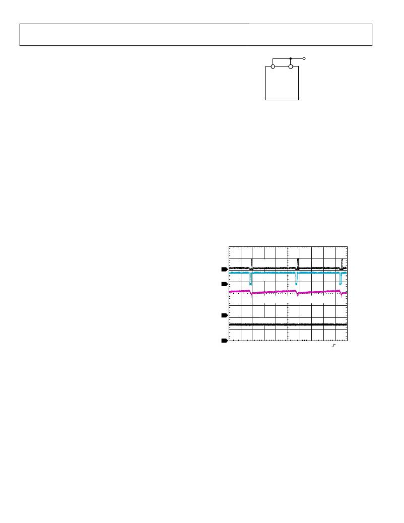
�OVERVOLTAGE� PROTECTION�
�The� ADP1850� has� a� built-in� circuit� for� detecting� output� over-�
�voltage� at� the� FB� node.� When� the� FB� voltage,� V� FB� ,� rises� above�
�the� overvoltage� threshold,� the� low-side� N-channel� MOSFET�
�(NMOSFET)� is� immediately� turned� on,� and� the� high-side�
�NMOSFET� is� turned� off� until� the� V� FB� drops� below� the�
�undervoltage� threshold.� This� action� is� known� as� the� crow-�
�bar� overvoltage� protection.� If� the� overvoltage� condition� is�
�not� removed,� the� controller� maintains� the� feedback� voltage�
�between� the� overvoltage� and� undervoltage� thresholds,� and� the�
�output� is� regulated� to� within� typically� +8%� and� ?8%� of� the�
�regulation� voltage.� During� an� overvoltage� event,� the� SS� node�
�discharges� toward� zero� through� an� internal� 3� k� pull-down�
�resistor.� When� the� voltage� at� FBx� drops� below� the� undervoltage�
�threshold,� the� soft� start� sequence� restarts.� Figure� 27� shows� the�
�overvoltage� protection� scheme� in� action� in� PSM.�
�DH1�
�1�
�PGOOD1�
�2�
�VO1� =� 1.8V� SHORTED� TO� 2V� SOURCE�
�3�
�VIN�
�cycle.� The� LDO� has� been� optimized� to� handle� these� transients�
�without� overload� faults.� Due� to� the� gate� drive� loading,� using� the�
�VCCO� output� for� other� external� auxiliary� system� loads� is� not�
�recommended.�
�4�
�CH1� 20.0V� CH2� 5.00V� M100μs� A� CH1�
�CH3� 1.00V� CH4� 10.0V�
�Figure� 27.� Overvoltage� Protection� in� PSM�
�10.0V�
�The� LDO� includes� a� current� limit� well� above� the� expected�
�maximum� gate� drive� load.� This� current� limit� also� includes� a�
�short-circuit� fold� back� to� further� limit� the� VCCO� current� in� the�
�event� of� a� short-circuit� fault.�
�The� VDL� pin� provides� power� to� the� low-side� driver.� Connect�
�VDL� to� VCCO.� Bypass� VDL� to� PGNDx� with� a� 1� μF� (minimum)�
�ceramic� capacitor,� which� must� be� placed� close� to� the� VDL� pin.�
�For� an� input� voltage� less� than� 5.5� V,� it� is� recommended� to�
�bypass� the� LDO� by� connecting� VIN� to� VCCO,� as� shown� in�
��the� input� range� is� 4� V� to� 7� V,� the� LDO� cannot� be� bypassed� by�
�POWER� GOOD�
�The� PGOODx� pin� is� an� open-drain� NMOSFET� with� an� internal�
�12� k� pull-up� resistor� connected� between� PGOODx� and� VCCO.�
�PGOODx� is� internally� pulled� up� to� VCCO� during� normal�
�operation� and� is� active� low� when� tripped.� When� the� feedback�
�voltage,� V� FB� ,� rises� above� the� overvoltage� threshold� or� drops�
�below� the� undervoltage� threshold,� the� PGOODx� output� is�
�pulled� to� ground� after� a� delay� of� 12� μs.� The� overvoltage� or�
�undervoltage� condition� must� exist� for� more� than� 10� μs� for�
�PGOODx� to� become� active.� The� PGOODx� output� also�
�becomes� active� if� a� thermal� overload� condition� is� detected.�
�shorting� VIN� to� VCCO� because� the� 7� V� input� has� exceeded� the�
�maximum� voltage� rating� of� the� VCCO� pin.� In� this� case,� use� the�
�LDO� to� drive� the� internal� drivers,� but� keep� in� mind� that� there� is�
�a� dropout� when� V� IN� is� less� than� 5� V.�
�Rev.� A� |� Page� 14� of� 32�
�相关PDF资料 |
PDF描述 |
|---|---|
| SS2P2LHE3/84A | DIODE SCHOTTKY 2A 20V SMP |
| SS3P6LHM3/87A | DIODE SCHOTTKY 3A 60V SMP |
| ADP2114-EVALZ | BOARD EVALUATION 3.3V/1.8V |
| RCM12DCBI-S189 | CONN EDGECARD 24POS R/A .156 SLD |
| GCC28DCAD | CONN EDGECARD 56POS R/A .100 SLD |
相关代理商/技术参数 |
参数描述 |
|---|---|
| ADP1850SP-EVALZ | 功能描述:EVAL BOARD FOR ADP1850SP RoHS:是 类别:编程器,开发系统 >> 评估板 - DC/DC 与 AC/DC(离线)SMPS 系列:- 产品培训模块:Obsolescence Mitigation Program 标准包装:1 系列:True Shutdown™ 主要目的:DC/DC,步升 输出及类型:1,非隔离 功率 - 输出:- 输出电压:- 电流 - 输出:1A 输入电压:2.5 V ~ 5.5 V 稳压器拓扑结构:升压 频率 - 开关:3MHz 板类型:完全填充 已供物品:板 已用 IC / 零件:MAX8969 |
| ADP1851ACPZ-R7 | 功能描述:电流型 PWM 控制器 w-range input Synch StepDown DC/DC Cntr RoHS:否 制造商:Texas Instruments 开关频率:27 KHz 上升时间: 下降时间: 工作电源电压:6 V to 15 V 工作电源电流:1.5 mA 输出端数量:1 最大工作温度:+ 105 C 安装风格:SMD/SMT 封装 / 箱体:TSSOP-14 |
| ADP1851-EVALZ | 功能描述:电源管理IC开发工具 Evaluation Board 1.8V 25A Output RoHS:否 制造商:Maxim Integrated 产品:Evaluation Kits 类型:Battery Management 工具用于评估:MAX17710GB 输入电压: 输出电压:1.8 V |
| ADP1853 | 制造商:AD 制造商全称:Analog Devices 功能描述:Synchronous, Step-Down DC-to-DC Controller |
| ADP1853ACPZ-R7 | 功能描述:DC/DC 开关控制器 Synch StepDown DC/DC Cntr w/Volt trking RoHS:否 制造商:Texas Instruments 输入电压:6 V to 100 V 开关频率: 输出电压:1.215 V to 80 V 输出电流:3.5 A 输出端数量:1 最大工作温度:+ 125 C 安装风格: 封装 / 箱体:CPAK |
发布紧急采购,3分钟左右您将得到回复。