- 您现在的位置:买卖IC网 > PDF目录17412 > ADP1850DP-EVALZ (Analog Devices Inc)EVAL BOARD FOR ADP1850DP PDF资料下载
参数资料
| 型号: | ADP1850DP-EVALZ |
| 厂商: | Analog Devices Inc |
| 文件页数: | 18/32页 |
| 文件大小: | 0K |
| 描述: | EVAL BOARD FOR ADP1850DP |
| 标准包装: | 1 |
| 主要目的: | DC/DC,步降 |
| 输出及类型: | 1,非隔离 |
| 输出电压: | 1.09V |
| 电流 - 输出: | 50A |
| 输入电压: | 10 ~ 15 V |
| 稳压器拓扑结构: | 降压 |
| 频率 - 开关: | 300kHz |
| 板类型: | 完全填充 |
| 已供物品: | 板 |
| 已用 IC / 零件: | ADP1850DP |
第1页第2页第3页第4页第5页第6页第7页第8页第9页第10页第11页第12页第13页第14页第15页第16页第17页当前第18页第19页第20页第21页第22页第23页第24页第25页第26页第27页第28页第29页第30页第31页第32页
�� �
�
�ADP1850�
�INPUT� CAPACITOR� SELECTION�
�The� input� current� to� a� buck� converter� is� a� pulse� waveform.� It� is�
�zero� when� the� high-side� switch� is� off� and� approximately� equal�
�to� the� load� current� when� it� is� on.� The� input� capacitor� carries� the�
�input� ripple� current,� allowing� the� input� power� source� to� supply�
�only� the� direct� current.� The� input� capacitor� needs� sufficient�
�ripple� current� rating� to� handle� the� input� ripple,� as� well� as� an�
�ESR� that� is� low� enough� to� mitigate� input� voltage� ripple.� For� the�
�usual� current� ranges� for� these� converters,� it� is� good� practice� to�
�use� two� parallel� capacitors� placed� close� to� the� drains� of� the�
�high-side� switch� MOSFETs� (one� bulk� capacitor� of� sufficiently�
�high� current� rating� and� a� 10� μF� ceramic� decoupling� capacitor,�
�typically).�
�Select� an� input� bulk� capacitor� based� on� its� ripple� current� rating.�
�Data� Sheet�
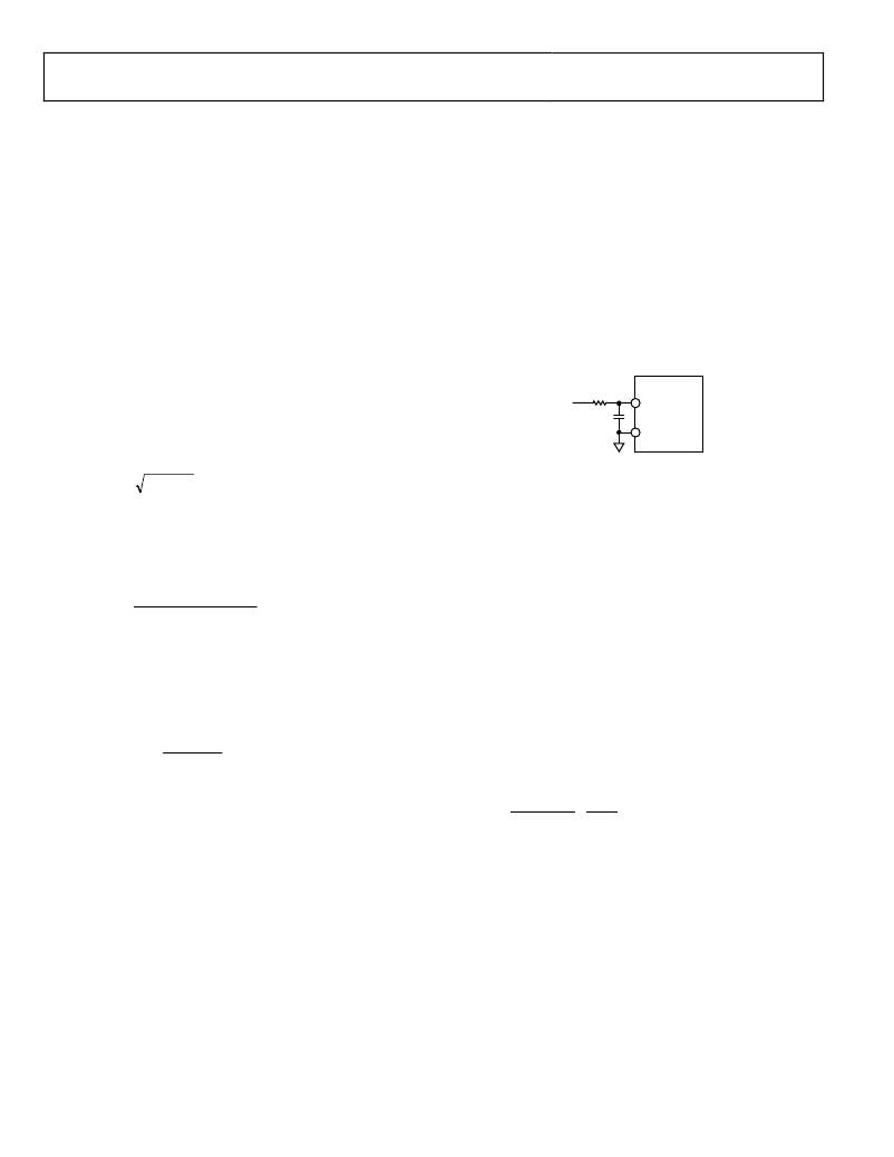
�INPUT� FILTER�
�Normally� a� 0.1� μF� or� greater� value� bypass� capacitor� from� the�
�input� pin� (VIN)� to� AGND� is� sufficient� for� filtering� out� any�
�unwanted� switching� noise.� However,� depending� on� the� PCB�
�layout,� some� switching� noise� can� enter� the� ADP1850� internal�
�circuitry;� therefore,� it� is� recommended� to� have� a� low� pass� filter�
�at� the� VIN� pin.� Connecting� a� resistor,� between� 2� Ω� and� 5� Ω,� in�
�series� with� VIN� and� a� 1� μF� ceramic� capacitor� between� VIN� and�
�AGND� creates� a� low� pass� filter� that� effectively� filters� out� any�
�unwanted� glitches� caused� by� the� switching� regulator.� Keep� in�
�mind� that� the� input� current� could� be� larger� than� 100� mA� when�
�driving� large� MOSFETs.� A� 100� mA� across� a� 5� Ω� resistor� creates�
�a� 0.5� V� drop,� which� is� the� same� voltage� drop� in� VCCO.� In� this�
�case,� a� lower� resistor� value� is� desirable.�
�D� =�
�First,� determine� the� duty� cycle� of� the� output.�
�V� OUT�
�V� IN�
�V� IN�
�2� ?� TO� 5� ?�
�1μF�
�ADP1850�
�VIN�
�AGND�
�I� O� � D� (� 1� ?� D� )�
�(� V� PP� ?� I� O� � DR� ESR� )� f� SW�
�C� IN� ,� MIN� =� I� O� �
�V� IN� ?� V� OUT� V�
�The� input� capacitor� RMS� ripple� current� is� given� by�
�I� RMS� =� I� O� D� (� 1� ?� D� )�
�where:�
�I� O� is� the� output� current.�
�D� is� the� duty� cycle�
�The� minimum� input� capacitance� required� for� a� particular� load� is�
�C� IN� ,� MIN� =�
�where:�
�V� PP� is� the� desired� input� ripple� voltage.�
�R� ESR� is� the� equivalent� series� resistance� of� the� capacitor.�
�If� an� MLCC� capacitor� is� used,� the� ESR� is� near� 0,� then� the�
�equation� is� simplified� to�
�D� (� 1� ?� D� )�
�V� PP� � f� SW�
�The� capacitance� of� MLCC� is� voltage� dependent.� The� actual�
�capacitance� of� the� selected� capacitor� must� be� derated� according� to�
�the� manufacturer’s� specification.� In� addition,� add� more� bulk�
�capacitance,� such� as� by� using� electrolytic� or� polymer� capacitors,�
�as� necessary� for� large� step� load� transients.� Make� sure� the�
�current� ripple� rating� of� the� bulk� capacitor� exceeds� the�
�maximum� input� current� ripple� of� a� particular� design.�
�Figure� 32.� Input� Filter� Configuration�
�BOOST� CAPACITOR� SELECTION�
�To� lower� system� component� count� and� cost,� the� ADP1850� has�
�an� integrated� rectifier� (equivalent� to� the� boost� diode)� between�
�VCCO� and� BSTx.� Choose� a� boost� ceramic� capacitor� with� a�
�value� between� 0.1� μF� and� 0.22� μF;� this� capacitor� provides� the�
�current� for� the� high-side� driver� during� switching.�
�INDUCTOR� SELECTION�
�The� output� LC� filter� smoothes� the� switched� voltage� at� SWx.� For�
�most� applications,� choose� an� inductor� value� such� that� the�
�inductor� ripple� current� is� between� 20%� and� 40%� of� the�
�maximum� dc� output� load� current.� Generally,� a� larger� inductor�
�current� ripple� generates� more� power� loss� in� the� inductor� and�
�larger� voltage� ripples� at� the� output.� Check� the� inductor� data�
�sheet� to� make� sure� that� the� saturation� current� of� the� inductor� is�
�well� above� the� peak� inductor� current� of� a� particular� design.�
�Choose� the� inductor� value� by� the� following� equation:�
�L� =� � OUT�
�f� SW� ×� Δ� I� L� V� IN�
�where:�
�L� is� the� inductor� value.�
�f� SW� is� the� switching� frequency.�
�V� OUT� is� the� output� voltage.�
�V� IN� is� the� input� voltage.�
�Δ� I� L� is� the� peak-to-peak� inductor� ripple� current.�
�Rev.� A� |� Page� 18� of� 32�
�相关PDF资料 |
PDF描述 |
|---|---|
| SS2P2LHE3/84A | DIODE SCHOTTKY 2A 20V SMP |
| SS3P6LHM3/87A | DIODE SCHOTTKY 3A 60V SMP |
| ADP2114-EVALZ | BOARD EVALUATION 3.3V/1.8V |
| RCM12DCBI-S189 | CONN EDGECARD 24POS R/A .156 SLD |
| GCC28DCAD | CONN EDGECARD 56POS R/A .100 SLD |
相关代理商/技术参数 |
参数描述 |
|---|---|
| ADP1850SP-EVALZ | 功能描述:EVAL BOARD FOR ADP1850SP RoHS:是 类别:编程器,开发系统 >> 评估板 - DC/DC 与 AC/DC(离线)SMPS 系列:- 产品培训模块:Obsolescence Mitigation Program 标准包装:1 系列:True Shutdown™ 主要目的:DC/DC,步升 输出及类型:1,非隔离 功率 - 输出:- 输出电压:- 电流 - 输出:1A 输入电压:2.5 V ~ 5.5 V 稳压器拓扑结构:升压 频率 - 开关:3MHz 板类型:完全填充 已供物品:板 已用 IC / 零件:MAX8969 |
| ADP1851ACPZ-R7 | 功能描述:电流型 PWM 控制器 w-range input Synch StepDown DC/DC Cntr RoHS:否 制造商:Texas Instruments 开关频率:27 KHz 上升时间: 下降时间: 工作电源电压:6 V to 15 V 工作电源电流:1.5 mA 输出端数量:1 最大工作温度:+ 105 C 安装风格:SMD/SMT 封装 / 箱体:TSSOP-14 |
| ADP1851-EVALZ | 功能描述:电源管理IC开发工具 Evaluation Board 1.8V 25A Output RoHS:否 制造商:Maxim Integrated 产品:Evaluation Kits 类型:Battery Management 工具用于评估:MAX17710GB 输入电压: 输出电压:1.8 V |
| ADP1853 | 制造商:AD 制造商全称:Analog Devices 功能描述:Synchronous, Step-Down DC-to-DC Controller |
| ADP1853ACPZ-R7 | 功能描述:DC/DC 开关控制器 Synch StepDown DC/DC Cntr w/Volt trking RoHS:否 制造商:Texas Instruments 输入电压:6 V to 100 V 开关频率: 输出电压:1.215 V to 80 V 输出电流:3.5 A 输出端数量:1 最大工作温度:+ 125 C 安装风格: 封装 / 箱体:CPAK |
发布紧急采购,3分钟左右您将得到回复。