- 您现在的位置:买卖IC网 > PDF目录19383 > ADSP-21368KBPZ-2A (Analog Devices Inc)IC DSP 32BIT 333MHZ 256-BGA PDF资料下载
参数资料
| 型号: | ADSP-21368KBPZ-2A |
| 厂商: | Analog Devices Inc |
| 文件页数: | 11/64页 |
| 文件大小: | 0K |
| 描述: | IC DSP 32BIT 333MHZ 256-BGA |
| 产品培训模块: | SHARC Processor Overview |
| 标准包装: | 1 |
| 系列: | SHARC® |
| 类型: | 浮点 |
| 接口: | DAI,DPI |
| 时钟速率: | 333MHz |
| 非易失内存: | ROM(768 kB) |
| 芯片上RAM: | 256kB |
| 电压 - 输入/输出: | 3.30V |
| 电压 - 核心: | 1.20V |
| 工作温度: | 0°C ~ 70°C |
| 安装类型: | 表面贴装 |
| 封装/外壳: | 256-LBGA 裸露焊盘 |
| 供应商设备封装: | 256-BGA(27x27) |
| 包装: | 托盘 |
第1页第2页第3页第4页第5页第6页第7页第8页第9页第10页当前第11页第12页第13页第14页第15页第16页第17页第18页第19页第20页第21页第22页第23页第24页第25页第26页第27页第28页第29页第30页第31页第32页第33页第34页第35页第36页第37页第38页第39页第40页第41页第42页第43页第44页第45页第46页第47页第48页第49页第50页第51页第52页第53页第54页第55页第56页第57页第58页第59页第60页第61页第62页第63页第64页
Rev. F
|
Page 19 of 64
|
October 2013
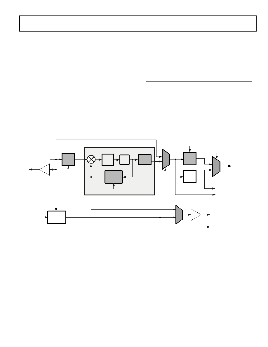
The product of CLKIN and PLLM must never exceed fVCO
(max) in Table 13 if the input divider is enabled
(INDIV = 1).
The VCO frequency is calculated as follows:
fVCO = 2 PLLM fINPUT
fCCLK = (2 PLLM fINPUT) (2 PLLD)
where:
fVCO = VCO output
PLLM = Multiplier value programmed in the PMCTL register.
During reset, the PLLM value is derived from the ratio selected
using the CLK_CFG pins in hardware.
PLLD = Divider value 1, 2, 4, or 8 based on the PLLD value pro-
grammed on the PMCTL register. During reset this value is 1.
fINPUT = Input frequency to the PLL.
fINPUT = CLKIN when the input divider is disabled or
fINPUT = CLKIN 2 when the input divider is enabled
Note the definitions of the clock periods that are a function of
CLKIN and the appropriate ratio control shown in and
Table 11. All of the timing specifications for the ADSP-2136x
peripherals are defined in relation to t
PCLK. See the peripheral spe-
cific timing section for each peripheral’s timing information.
Figure 5 shows core to CLKIN relationships with external oscil-
lator or crystal. The shaded divider/multiplier blocks denote
where clock ratios can be set through hardware or software
using the power management control register (PMCTL). For
more information, see the processor hardware reference.
Table 11. Clock Periods
Timing
Requirements
Description
t
CK
CLKIN Clock Period
t
CCLK
Processor Core Clock Period
t
PCLK
Peripheral Clock Period = 2 × t
CCLK
Figure 5. Core Clock and System Clock Relationship to CLKIN
LOOP
FILTER
CLKIN
PCLK
SDCLK
SDRAM
DIVIDER
PMCTL
(PLLBP)
B
Y
P
A
S
M
U
X
DIVIDE
BY 2
PMCTL
(SDCKR)
CCLK
B
Y
P
A
S
M
U
X
PLL
XTAL
CLKIN
DIVIDER
PLL
MULTIPLIER
BUF
VCO
BUF
PMCTL
(INDIV)
PLL
DIVIDER
CLK_CFGx/PMCTL (2xPLLM)
P
IN
M
U
X
CLKOUT (TESTONLY)
DELAY OF
4096 CLKIN
CYCLES
CCLK
PCLK
PMCTL
(PLLBP)
PMCTL
(2xPLLD)
fVCO
fCCLK
fINPUT
相关PDF资料 |
PDF描述 |
|---|---|
| MC79M15CT | IC REG LDO -15V .5A TO220AB |
| TLJR336M004R3000 | CAP TANT 33UF 4V 20% 0805 |
| VI-21T-CW-F4 | CONVERTER MOD DC/DC 6.5V 100W |
| MC79M12CT | IC REG LDO -12V .5A TO220AB |
| VI-2NT-CY-F1 | CONVERTER MOD DC/DC 6.5V 50W |
相关代理商/技术参数 |
参数描述 |
|---|---|
| ADSP-21368KBPZ-3A | 功能描述:IC DSP 32BIT 400MHZ 256BGA RoHS:是 类别:集成电路 (IC) >> 嵌入式 - DSP(数字式信号处理器) 系列:SHARC® 标准包装:2 系列:StarCore 类型:SC140 内核 接口:DSI,以太网,RS-232 时钟速率:400MHz 非易失内存:外部 芯片上RAM:1.436MB 电压 - 输入/输出:3.30V 电压 - 核心:1.20V 工作温度:-40°C ~ 105°C 安装类型:表面贴装 封装/外壳:431-BFBGA,FCBGA 供应商设备封装:431-FCPBGA(20x20) 包装:托盘 |
| ADSP-21368SKBP-ENG | 制造商:AD 制造商全称:Analog Devices 功能描述:Preliminary Technical Data |
| ADSP-21368SKBPZENG | 制造商:AD 制造商全称:Analog Devices 功能描述:Preliminary Technical Data |
| ADSP-21369 | 制造商:AD 制造商全称:Analog Devices 功能描述:The ADSP-21367/ADSP-21368/ADSP-21369 are available with a 400 MHz core instruction rate with unique audiocentric peripherals such as the digital audio interface, S/PDIF transceiver, serial ports, 8-channel asynchronous sample rate converter, precision clock generators, and more. |
| ADSP-21369BBP-2A | 功能描述:IC DSP 32BIT 333MHZ 256-BGA RoHS:否 类别:集成电路 (IC) >> 嵌入式 - DSP(数字式信号处理器) 系列:SHARC® 标准包装:2 系列:StarCore 类型:SC140 内核 接口:DSI,以太网,RS-232 时钟速率:400MHz 非易失内存:外部 芯片上RAM:1.436MB 电压 - 输入/输出:3.30V 电压 - 核心:1.20V 工作温度:-40°C ~ 105°C 安装类型:表面贴装 封装/外壳:431-BFBGA,FCBGA 供应商设备封装:431-FCPBGA(20x20) 包装:托盘 |
发布紧急采购,3分钟左右您将得到回复。