- 您现在的位置:买卖IC网 > PDF目录19383 > ADSP-21368KBPZ-2A (Analog Devices Inc)IC DSP 32BIT 333MHZ 256-BGA PDF资料下载
参数资料
| 型号: | ADSP-21368KBPZ-2A |
| 厂商: | Analog Devices Inc |
| 文件页数: | 47/64页 |
| 文件大小: | 0K |
| 描述: | IC DSP 32BIT 333MHZ 256-BGA |
| 产品培训模块: | SHARC Processor Overview |
| 标准包装: | 1 |
| 系列: | SHARC® |
| 类型: | 浮点 |
| 接口: | DAI,DPI |
| 时钟速率: | 333MHz |
| 非易失内存: | ROM(768 kB) |
| 芯片上RAM: | 256kB |
| 电压 - 输入/输出: | 3.30V |
| 电压 - 核心: | 1.20V |
| 工作温度: | 0°C ~ 70°C |
| 安装类型: | 表面贴装 |
| 封装/外壳: | 256-LBGA 裸露焊盘 |
| 供应商设备封装: | 256-BGA(27x27) |
| 包装: | 托盘 |
第1页第2页第3页第4页第5页第6页第7页第8页第9页第10页第11页第12页第13页第14页第15页第16页第17页第18页第19页第20页第21页第22页第23页第24页第25页第26页第27页第28页第29页第30页第31页第32页第33页第34页第35页第36页第37页第38页第39页第40页第41页第42页第43页第44页第45页第46页当前第47页第48页第49页第50页第51页第52页第53页第54页第55页第56页第57页第58页第59页第60页第61页第62页第63页第64页
Rev. F
|
Page 51 of 64
|
October 2013
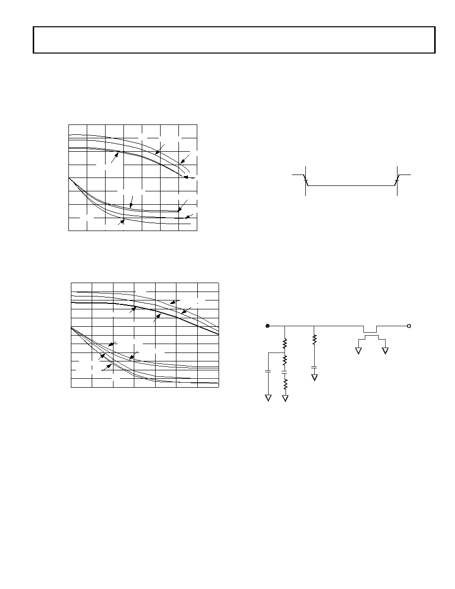
OUTPUT DRIVE CURRENTS
Figure 39 shows typical I-V characteristics for the output driv-
ers and Figure 40 shows typical I-V characteristics for the
SDCLK output drivers. The curves represent the current drive
capability of the output drivers as a function of output voltage.
TEST CONDITIONS
The ac signal specifications (timing parameters) appear in
Table 14 on Page 23 through Table 42 on Page 50. These include
output disable time, output enable time, and capacitive loading.
The timing specifications for the SHARC apply for the voltage
reference levels in Figure 41.
Timing is measured on signals when they cross the 1.5 V level as
described in Figure 41. All delays (in nanoseconds) are mea-
sured between the point that the first signal reaches 1.5 V and
the point that the second signal reaches 1.5 V.
CAPACITIVE LOADING
Output delays and holds are based on standard capacitive loads
of an average of 6 pF on all pins (see Figure 42). Figure 47 and
Figure 48 show graphically how output delays and holds vary
with load capacitance. The graphs of Figure 43 through
Figure 48 may not be linear outside the ranges shown for Typi-
cal Output Delay vs. Load Capacitance and Typical Output Rise
Time (20% to 80%, V = Min) vs. Load Capacitance.
Figure 39. Typical Drive at Junction Temperature
Figure 40. SDCLK1–0 Drive at Junction Temperature
SWEEP (VDDEXT) VOLTAGE (V)
-
20
0
3.5
0.5
1.0
1.5
2.0
2.5
3.0
0
-
40
-
30
20
40
-
10
S
O
U
R
C
E
(V
D
E
X
T
)
C
U
R
E
N
T
(m
A
)
VOL
3.11V, 125°C
3.3V, 25°C
3.47V, -45°C
VOH
30
10
3.11V, 125°C
3.3V, 25°C
3.47V, -45°C
3.11V, 105°C
-
60
0
3.5
0.5
1.0
1.5
2.0
2.5
3.0
0
-
45
-
30
60
75
-
15
S
O
U
R
C
E
(V
D
E
X
T
)
C
U
R
E
N
T
(m
A
)
VOL
3 .1 3 V, 12 5 °C
3.3 V, 25 °C
3 .47 V, -45 °C
V
OH
3.1 3V, 1 05 °C
45
-
90
-
75
-
105
30
15
3.1 3V, 1 25 °C
3.3 V, 2 5°C
3 .47 V, -45°C
3 .1 3 V, 10 5° C
S WEE P (VDDEXT)VOLTAG E (V)
Figure 41. Voltage Reference Levels for AC Measurements
Figure 42. Equivalent Device Loading for AC Measurements
(Includes All Fixtures)
INPUT
OR
OUTPUT
1.5V
T1
ZO = 50
Ω (impedance)
TD = 4.04
± 1.18 ns
2pF
TESTER PIN ELECTRONICS
50
Ω
0.5pF
70
Ω
400
Ω
45
Ω
4pF
NOTES:
THE WORST CASE TRANSMISSION LINE DELAY IS SHOWN AND CAN BE USED
FOR THE OUTPUT TIMING ANALYSIS TO REFELECT THE TRANSMISSION LINE
EFFECT AND MUST BE CONSIDERED. THE TRANSMISSION LINE (TD), IS FOR
LOAD ONLY AND DOES NOT AFFECT THE DATA SHEET TIMING SPECIFICATIONS.
ANALOG DEVICES RECOMMENDS USING THE IBIS MODEL TIMING FOR A GIVEN
SYSTEM REQUIREMENT. IF NECESSARY, A SYSTEM MAY INCORPORATE
EXTERNAL DRIVERS TO COMPENSATE FOR ANY TIMING DIFFERENCES.
1.5V
DUT
OUTPUT
相关PDF资料 |
PDF描述 |
|---|---|
| MC79M15CT | IC REG LDO -15V .5A TO220AB |
| TLJR336M004R3000 | CAP TANT 33UF 4V 20% 0805 |
| VI-21T-CW-F4 | CONVERTER MOD DC/DC 6.5V 100W |
| MC79M12CT | IC REG LDO -12V .5A TO220AB |
| VI-2NT-CY-F1 | CONVERTER MOD DC/DC 6.5V 50W |
相关代理商/技术参数 |
参数描述 |
|---|---|
| ADSP-21368KBPZ-3A | 功能描述:IC DSP 32BIT 400MHZ 256BGA RoHS:是 类别:集成电路 (IC) >> 嵌入式 - DSP(数字式信号处理器) 系列:SHARC® 标准包装:2 系列:StarCore 类型:SC140 内核 接口:DSI,以太网,RS-232 时钟速率:400MHz 非易失内存:外部 芯片上RAM:1.436MB 电压 - 输入/输出:3.30V 电压 - 核心:1.20V 工作温度:-40°C ~ 105°C 安装类型:表面贴装 封装/外壳:431-BFBGA,FCBGA 供应商设备封装:431-FCPBGA(20x20) 包装:托盘 |
| ADSP-21368SKBP-ENG | 制造商:AD 制造商全称:Analog Devices 功能描述:Preliminary Technical Data |
| ADSP-21368SKBPZENG | 制造商:AD 制造商全称:Analog Devices 功能描述:Preliminary Technical Data |
| ADSP-21369 | 制造商:AD 制造商全称:Analog Devices 功能描述:The ADSP-21367/ADSP-21368/ADSP-21369 are available with a 400 MHz core instruction rate with unique audiocentric peripherals such as the digital audio interface, S/PDIF transceiver, serial ports, 8-channel asynchronous sample rate converter, precision clock generators, and more. |
| ADSP-21369BBP-2A | 功能描述:IC DSP 32BIT 333MHZ 256-BGA RoHS:否 类别:集成电路 (IC) >> 嵌入式 - DSP(数字式信号处理器) 系列:SHARC® 标准包装:2 系列:StarCore 类型:SC140 内核 接口:DSI,以太网,RS-232 时钟速率:400MHz 非易失内存:外部 芯片上RAM:1.436MB 电压 - 输入/输出:3.30V 电压 - 核心:1.20V 工作温度:-40°C ~ 105°C 安装类型:表面贴装 封装/外壳:431-BFBGA,FCBGA 供应商设备封装:431-FCPBGA(20x20) 包装:托盘 |
发布紧急采购,3分钟左右您将得到回复。