- 您现在的位置:买卖IC网 > PDF目录11199 > ADUC7036BCPZ (Analog Devices Inc)IC MCU FLASH 96K ANLGI/O 48LFCSP PDF资料下载
参数资料
| 型号: | ADUC7036BCPZ |
| 厂商: | Analog Devices Inc |
| 文件页数: | 102/132页 |
| 文件大小: | 0K |
| 描述: | IC MCU FLASH 96K ANLGI/O 48LFCSP |
| 产品培训模块: | Process Control |
| 标准包装: | 1 |
| 系列: | MicroConverter® ADuC7xxx |
| 核心处理器: | ARM7 |
| 芯体尺寸: | 16/32-位 |
| 速度: | 20.48MHz |
| 连通性: | LIN,SPI,UART/USART |
| 外围设备: | PSM,温度传感器,WDT |
| 输入/输出数: | 9 |
| 程序存储器容量: | 96KB(48K x 16) |
| 程序存储器类型: | 闪存 |
| RAM 容量: | 1.5K x 32 |
| 电压 - 电源 (Vcc/Vdd): | 3.5 V ~ 18 V |
| 数据转换器: | A/D 2x16b |
| 振荡器型: | 内部 |
| 工作温度: | -40°C ~ 115°C |
| 封装/外壳: | 48-VFQFN 裸露焊盘,CSP |
| 包装: | 托盘 |
第1页第2页第3页第4页第5页第6页第7页第8页第9页第10页第11页第12页第13页第14页第15页第16页第17页第18页第19页第20页第21页第22页第23页第24页第25页第26页第27页第28页第29页第30页第31页第32页第33页第34页第35页第36页第37页第38页第39页第40页第41页第42页第43页第44页第45页第46页第47页第48页第49页第50页第51页第52页第53页第54页第55页第56页第57页第58页第59页第60页第61页第62页第63页第64页第65页第66页第67页第68页第69页第70页第71页第72页第73页第74页第75页第76页第77页第78页第79页第80页第81页第82页第83页第84页第85页第86页第87页第88页第89页第90页第91页第92页第93页第94页第95页第96页第97页第98页第99页第100页第101页当前第102页第103页第104页第105页第106页第107页第108页第109页第110页第111页第112页第113页第114页第115页第116页第117页第118页第119页第120页第121页第122页第123页第124页第125页第126页第127页第128页第129页第130页第131页第132页
ADuC7036
Rev. C | Page 71 of 132
TIMERS
The ADuC7036 features five general-purpose timer/counters.
Timer0, or the lifetime timer
Timer1, or general-purpose timer
Timer2, or the wake-up timer
Timer3, or the watchdog timer
Timer4, or the STI timer
The five timers in their normal mode of operation can be in
either free running mode or periodic mode.
Timers are started by writing data to the control register of the
corresponding timer (TxCON). The counting mode and speed
depend on the configuration chosen in TxCON.
In normal mode, an IRQ is generated each time the value of
the counter reaches 0 when counting down, or each time the
counter value reaches full scale when counting up. An IRQ
can be cleared by writing any value to clear the register of
that particular timer (TxCLRI).
The three timers in their normal mode of operation can be
either free-running or periodic.
In free-running mode, starting with the value in the TxLD
register, the counter decrements/increments from the maximum/
minimum value until zero/full scale and starts again at the
maximum/minimum value. This means that, in free-running
mode, TxVAL is not reloaded when the relevant interrupt bit is
set but the count simply rolls over as the counter underflows or
overflows.
In periodic mode, the counter decrements/increments from
the value in the load register (TxLD MMR) until zero/full scale
starts again from this value. This means when the relevant
interrupt bit is set, TxVAL is reloaded with TxLD and counting
starts again from this value.
Loading the TxLD register with zero is not recommended. The
value of a counter can be read at any time by accessing its value
register (TxVAL).
In addition, Timer0, Timer1, and Timer4 each have a capture
register (T0CAP, T1CAP, and T4CAP, respectively) that can
hold the value captured by an enabled IRQ event. The IRQ
events are described in Table 52.
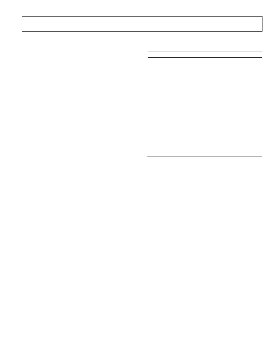
Table 52. Timer Event Capture
Bit
Description
0
Timer0, or the lifetime timer
1
Timer1, or general-purpose timer
2
Timer2, or the wake-up timer
3
Timer3, or the watchdog timer
4
Timer4, or the STI timer
5
LIN hardware
6
Flash/EE interrupt
7
PLL lock
8
ADC
9
UART
10
SPI master
11
XIRQ0 (GPIO_0)
12
XIRQ1 (GPIO_5)
13
Reserved
14
IRQ3 high voltage interrupt
15
SPI slave
16
XIRQ4 (GPIO_7); see the General-Purpose I/O section
17
XIRQ5 (GPIO_8); see the General-Purpose I/O section
SYNCHRONIZATION OF TIMERS ACROSS
ASYNCHRONOUS CLOCK DOMAINS
The block diagram in Figure 33 shows the interface between
user timer MMRs and the core timer blocks. User code can
access all timer MMRs directly, including TxLD, TxVAL,
TxCON, and TxCLRI. Data must then transfer from these
MMRs to the core timers (T0, T1, T2, T3, and T4) within the
timer subsystem. Theses core timers are buffered from the
user MMR interface by the synchronization (SYNC) block.
The principal of the SYNC block is to provide a method that
ensures that data and other required control signals can cross
asynchronous clock domains correctly. An example of asyn-
chronous clock domains is the MCU running on the 10 MHz
core clock, and Timer2 running on the low power oscillator of
32 kHz.
相关PDF资料 |
PDF描述 |
|---|---|
| ATSAM3X4EA-AU | IC MCU 2X128KB CORTEX-M3 144-QFP |
| AT91SAM7X128C-AU | IC MCU 32BIT 128KB FLASH 100LQFP |
| NC7WB66L8X | IC SWITCH DUAL SPST-NO 8MICROPAK |
| MC74HCT4051ADR2G | ANALOG MULTIPLEXERS/DEMU SOIC16 |
| VE-B4P-IX | CONVERTER MOD DC/DC 13.8V 75W |
相关代理商/技术参数 |
参数描述 |
|---|---|
| ADUC7036BCPZ-RL | 功能描述:IC SENSOR AUTO 96K FLASH 48LFCSP RoHS:是 类别:集成电路 (IC) >> 嵌入式 - 微控制器, 系列:MicroConverter® ADuC7xxx 标准包装:38 系列:Encore!® XP® 核心处理器:eZ8 芯体尺寸:8-位 速度:5MHz 连通性:IrDA,UART/USART 外围设备:欠压检测/复位,LED,POR,PWM,WDT 输入/输出数:16 程序存储器容量:4KB(4K x 8) 程序存储器类型:闪存 EEPROM 大小:- RAM 容量:1K x 8 电压 - 电源 (Vcc/Vdd):2.7 V ~ 3.6 V 数据转换器:- 振荡器型:内部 工作温度:-40°C ~ 105°C 封装/外壳:20-SOIC(0.295",7.50mm 宽) 包装:管件 其它名称:269-4116Z8F0413SH005EG-ND |
| ADUC7036CCPZ | 功能描述:IC MCU 96K FLASH DUAL 48LFCSP RoHS:是 类别:集成电路 (IC) >> 嵌入式 - 微控制器, 系列:MicroConverter® ADuC7xxx 标准包装:38 系列:Encore!® XP® 核心处理器:eZ8 芯体尺寸:8-位 速度:5MHz 连通性:IrDA,UART/USART 外围设备:欠压检测/复位,LED,POR,PWM,WDT 输入/输出数:16 程序存储器容量:4KB(4K x 8) 程序存储器类型:闪存 EEPROM 大小:- RAM 容量:1K x 8 电压 - 电源 (Vcc/Vdd):2.7 V ~ 3.6 V 数据转换器:- 振荡器型:内部 工作温度:-40°C ~ 105°C 封装/外壳:20-SOIC(0.295",7.50mm 宽) 包装:管件 其它名称:269-4116Z8F0413SH005EG-ND |
| ADUC7036CCPZ-RL | 功能描述:IC MCU 96K FLASH DUAL 48LFCSP RoHS:是 类别:集成电路 (IC) >> 嵌入式 - 微控制器, 系列:MicroConverter® ADuC7xxx 标准包装:38 系列:Encore!® XP® 核心处理器:eZ8 芯体尺寸:8-位 速度:5MHz 连通性:IrDA,UART/USART 外围设备:欠压检测/复位,LED,POR,PWM,WDT 输入/输出数:16 程序存储器容量:4KB(4K x 8) 程序存储器类型:闪存 EEPROM 大小:- RAM 容量:1K x 8 电压 - 电源 (Vcc/Vdd):2.7 V ~ 3.6 V 数据转换器:- 振荡器型:内部 工作温度:-40°C ~ 105°C 封装/外壳:20-SOIC(0.295",7.50mm 宽) 包装:管件 其它名称:269-4116Z8F0413SH005EG-ND |
| ADUC7036DCPZ | 功能描述:IC MCU 96K FLASH DUAL 48LFCSP RoHS:是 类别:集成电路 (IC) >> 嵌入式 - 微控制器, 系列:MicroConverter® ADuC7xxx 标准包装:38 系列:Encore!® XP® 核心处理器:eZ8 芯体尺寸:8-位 速度:5MHz 连通性:IrDA,UART/USART 外围设备:欠压检测/复位,LED,POR,PWM,WDT 输入/输出数:16 程序存储器容量:4KB(4K x 8) 程序存储器类型:闪存 EEPROM 大小:- RAM 容量:1K x 8 电压 - 电源 (Vcc/Vdd):2.7 V ~ 3.6 V 数据转换器:- 振荡器型:内部 工作温度:-40°C ~ 105°C 封装/外壳:20-SOIC(0.295",7.50mm 宽) 包装:管件 其它名称:269-4116Z8F0413SH005EG-ND |
| ADUC7036DCPZ-RL | 功能描述:IC MCU 96K FLASH DUAL 48LFCSP RoHS:是 类别:集成电路 (IC) >> 嵌入式 - 微控制器, 系列:MicroConverter® ADuC7xxx 标准包装:38 系列:Encore!® XP® 核心处理器:eZ8 芯体尺寸:8-位 速度:5MHz 连通性:IrDA,UART/USART 外围设备:欠压检测/复位,LED,POR,PWM,WDT 输入/输出数:16 程序存储器容量:4KB(4K x 8) 程序存储器类型:闪存 EEPROM 大小:- RAM 容量:1K x 8 电压 - 电源 (Vcc/Vdd):2.7 V ~ 3.6 V 数据转换器:- 振荡器型:内部 工作温度:-40°C ~ 105°C 封装/外壳:20-SOIC(0.295",7.50mm 宽) 包装:管件 其它名称:269-4116Z8F0413SH005EG-ND |
发布紧急采购,3分钟左右您将得到回复。