- 您现在的位置:买卖IC网 > PDF目录11199 > ADUC7036BCPZ (Analog Devices Inc)IC MCU FLASH 96K ANLGI/O 48LFCSP PDF资料下载
参数资料
| 型号: | ADUC7036BCPZ |
| 厂商: | Analog Devices Inc |
| 文件页数: | 47/132页 |
| 文件大小: | 0K |
| 描述: | IC MCU FLASH 96K ANLGI/O 48LFCSP |
| 产品培训模块: | Process Control |
| 标准包装: | 1 |
| 系列: | MicroConverter® ADuC7xxx |
| 核心处理器: | ARM7 |
| 芯体尺寸: | 16/32-位 |
| 速度: | 20.48MHz |
| 连通性: | LIN,SPI,UART/USART |
| 外围设备: | PSM,温度传感器,WDT |
| 输入/输出数: | 9 |
| 程序存储器容量: | 96KB(48K x 16) |
| 程序存储器类型: | 闪存 |
| RAM 容量: | 1.5K x 32 |
| 电压 - 电源 (Vcc/Vdd): | 3.5 V ~ 18 V |
| 数据转换器: | A/D 2x16b |
| 振荡器型: | 内部 |
| 工作温度: | -40°C ~ 115°C |
| 封装/外壳: | 48-VFQFN 裸露焊盘,CSP |
| 包装: | 托盘 |
第1页第2页第3页第4页第5页第6页第7页第8页第9页第10页第11页第12页第13页第14页第15页第16页第17页第18页第19页第20页第21页第22页第23页第24页第25页第26页第27页第28页第29页第30页第31页第32页第33页第34页第35页第36页第37页第38页第39页第40页第41页第42页第43页第44页第45页第46页当前第47页第48页第49页第50页第51页第52页第53页第54页第55页第56页第57页第58页第59页第60页第61页第62页第63页第64页第65页第66页第67页第68页第69页第70页第71页第72页第73页第74页第75页第76页第77页第78页第79页第80页第81页第82页第83页第84页第85页第86页第87页第88页第89页第90页第91页第92页第93页第94页第95页第96页第97页第98页第99页第100页第101页第102页第103页第104页第105页第106页第107页第108页第109页第110页第111页第112页第113页第114页第115页第116页第117页第118页第119页第120页第121页第122页第123页第124页第125页第126页第127页第128页第129页第130页第131页第132页
ADuC7036
Rev. C | Page 21 of 132
ARM7 Exceptions
The ARM7 supports five types of exceptions with a privileged
processing mode associated with each type. The five types of
exceptions are as follows:
Normal interrupt or IRQ. This is provided to service
general-purpose interrupt handling of internal and
external events.
Fast interrupt or FIQ. This is provided to service data
transfer or a communication channel with low latency.
FIQ has priority over IRQ.
Memory abort (prefetch and data).
Attempted execution of an undefined instruction.
Software interrupt (SWI) instruction that can be used to
make a call to an operating system.
Typically, the programmer defines interrupts as IRQ, but for
higher priority interrupts, the programmer can define interrupts
as the FIQ type.
The priority of these exceptions and vector address are listed in
Table 9. Exception Priorities and Vector Addresses
Priority
Exception
Address
1
Hardware reset
0x00
2
Memory abort (data)
0x10
3
FIQ
0x1C
4
IRQ
0x18
5
Memory abort (prefetch)
0x0C
6
0x08
6
0x04
1 A software interrupt and an undefined instruction exception have the same
priority and are mutually exclusive.
The list of exceptions in Table 9 are located from 0x00 to 0x1C,
with a reserved location at 0x14. This location is required to be
written with either 0x27011970 or the checksum of Page 0,
excluding Location 0x14. If this is not done, user code does not
execute and LIN download mode is entered.
ARM Registers
The ARM7TDMI has 16 standard registers. R0 to R12 are used
for data manipulation, R13 is the stack pointer, R14 is the link
register, and R15 is the program counter that indicates the
instruction currently being executed. The link register contains
the address from which the user has branched (if the branch
and link command was used) or the command during which an
exception occurred.
The stack pointer contains the current location of the stack. As
a general rule, on an ARM7TDMI, the stack starts at the top of
the available RAM area and descends using the area as required.
A separate stack is defined for each of the exceptions. The size of
each stack is user configurable and is dependent on the target
application. On the ADuC7036, the stack begins at 0x00040FFC
and descends. When programming using high level languages,
such as C, it is necessary to ensure that the stack does not overflow.
This is dependent on the performance of the compiler that is used.
When an exception occurs, some of the standard registers are
replaced with registers specific to the exception mode. All
exception modes have replacement banked registers for the
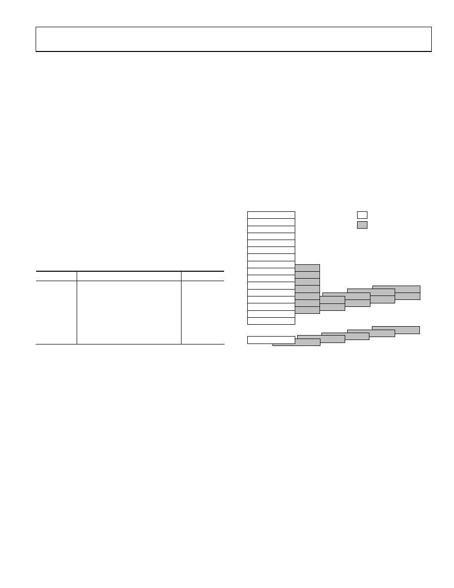
stack pointer (R13) and the link register (R14) as represented
in Figure 11. The FIQ mode has more registers (R8 to R12)
supporting faster interrupt processing. With the increased
number of noncritical registers, the interrupt can be processed
without the need to save or restore these registers, thereby
reducing the response time of the interrupt handling process.
More information relative to the model of the programmer and
the ARM7TDMI core architecture can be found in ARM7TDMI
technical and ARM architecture manuals available directly from
ARM Ltd.
USABLE IN USER MODE
SYSTEM MODES ONLY
SPSR_UND
SPSR_IRQ
SPSR_ABT
SPSR_SVC
R8_FIQ
R9_FIQ
R10_FIQ
R11_FIQ
R12_FIQ
R13_FIQ
R14_FIQ
R13_UND
R14_UND
R0
R1
R2
R3
R4
R5
R6
R7
R8
R9
R10
R11
R12
R13
R14
R15 (PC)
R13_IRQ
R14_IRQ
R13_ABT
R14_ABT
R13_SVC
R14_SVC
SPSR_FIQ
CPSR
USER MODE
FIQ
MODE
SVC
MODE
ABORT
MODE
IRQ
MODE
UNDEFINED
MODE
07
474
-01
1
Figure 11. Register Organization
Interrupt Latency
The worst-case latency for an FIQ consists of the longest possible
time for the request to pass through the synchronizer, for the
longest instruction to complete (the longest instruction is an LDM)
and load all the registers including the PC, and for the data abort
entry and the FIQ entry to complete. At the end of this time, the
ARM7TDMI executes the instruction at Address 0x1C (the FIQ
interrupt vector address). The maximum FIQ latency is 50 pro-
cessor cycles or just over 2.44 μs in a system using a continuous
20.48 MHz processor clock.
The maximum IRQ latency calculation is similar but must allow
for the fact that FIQ has higher priority and may delay entry into
the IRQ handling routine for an arbitrary length of time. This
time can be reduced to 42 cycles if the LDM command is not
used; some compilers have an option to compile without using
this command. Another option is to run the part in Thumb
mode, which reduces the time to 22 cycles.
相关PDF资料 |
PDF描述 |
|---|---|
| ATSAM3X4EA-AU | IC MCU 2X128KB CORTEX-M3 144-QFP |
| AT91SAM7X128C-AU | IC MCU 32BIT 128KB FLASH 100LQFP |
| NC7WB66L8X | IC SWITCH DUAL SPST-NO 8MICROPAK |
| MC74HCT4051ADR2G | ANALOG MULTIPLEXERS/DEMU SOIC16 |
| VE-B4P-IX | CONVERTER MOD DC/DC 13.8V 75W |
相关代理商/技术参数 |
参数描述 |
|---|---|
| ADUC7036BCPZ-RL | 功能描述:IC SENSOR AUTO 96K FLASH 48LFCSP RoHS:是 类别:集成电路 (IC) >> 嵌入式 - 微控制器, 系列:MicroConverter® ADuC7xxx 标准包装:38 系列:Encore!® XP® 核心处理器:eZ8 芯体尺寸:8-位 速度:5MHz 连通性:IrDA,UART/USART 外围设备:欠压检测/复位,LED,POR,PWM,WDT 输入/输出数:16 程序存储器容量:4KB(4K x 8) 程序存储器类型:闪存 EEPROM 大小:- RAM 容量:1K x 8 电压 - 电源 (Vcc/Vdd):2.7 V ~ 3.6 V 数据转换器:- 振荡器型:内部 工作温度:-40°C ~ 105°C 封装/外壳:20-SOIC(0.295",7.50mm 宽) 包装:管件 其它名称:269-4116Z8F0413SH005EG-ND |
| ADUC7036CCPZ | 功能描述:IC MCU 96K FLASH DUAL 48LFCSP RoHS:是 类别:集成电路 (IC) >> 嵌入式 - 微控制器, 系列:MicroConverter® ADuC7xxx 标准包装:38 系列:Encore!® XP® 核心处理器:eZ8 芯体尺寸:8-位 速度:5MHz 连通性:IrDA,UART/USART 外围设备:欠压检测/复位,LED,POR,PWM,WDT 输入/输出数:16 程序存储器容量:4KB(4K x 8) 程序存储器类型:闪存 EEPROM 大小:- RAM 容量:1K x 8 电压 - 电源 (Vcc/Vdd):2.7 V ~ 3.6 V 数据转换器:- 振荡器型:内部 工作温度:-40°C ~ 105°C 封装/外壳:20-SOIC(0.295",7.50mm 宽) 包装:管件 其它名称:269-4116Z8F0413SH005EG-ND |
| ADUC7036CCPZ-RL | 功能描述:IC MCU 96K FLASH DUAL 48LFCSP RoHS:是 类别:集成电路 (IC) >> 嵌入式 - 微控制器, 系列:MicroConverter® ADuC7xxx 标准包装:38 系列:Encore!® XP® 核心处理器:eZ8 芯体尺寸:8-位 速度:5MHz 连通性:IrDA,UART/USART 外围设备:欠压检测/复位,LED,POR,PWM,WDT 输入/输出数:16 程序存储器容量:4KB(4K x 8) 程序存储器类型:闪存 EEPROM 大小:- RAM 容量:1K x 8 电压 - 电源 (Vcc/Vdd):2.7 V ~ 3.6 V 数据转换器:- 振荡器型:内部 工作温度:-40°C ~ 105°C 封装/外壳:20-SOIC(0.295",7.50mm 宽) 包装:管件 其它名称:269-4116Z8F0413SH005EG-ND |
| ADUC7036DCPZ | 功能描述:IC MCU 96K FLASH DUAL 48LFCSP RoHS:是 类别:集成电路 (IC) >> 嵌入式 - 微控制器, 系列:MicroConverter® ADuC7xxx 标准包装:38 系列:Encore!® XP® 核心处理器:eZ8 芯体尺寸:8-位 速度:5MHz 连通性:IrDA,UART/USART 外围设备:欠压检测/复位,LED,POR,PWM,WDT 输入/输出数:16 程序存储器容量:4KB(4K x 8) 程序存储器类型:闪存 EEPROM 大小:- RAM 容量:1K x 8 电压 - 电源 (Vcc/Vdd):2.7 V ~ 3.6 V 数据转换器:- 振荡器型:内部 工作温度:-40°C ~ 105°C 封装/外壳:20-SOIC(0.295",7.50mm 宽) 包装:管件 其它名称:269-4116Z8F0413SH005EG-ND |
| ADUC7036DCPZ-RL | 功能描述:IC MCU 96K FLASH DUAL 48LFCSP RoHS:是 类别:集成电路 (IC) >> 嵌入式 - 微控制器, 系列:MicroConverter® ADuC7xxx 标准包装:38 系列:Encore!® XP® 核心处理器:eZ8 芯体尺寸:8-位 速度:5MHz 连通性:IrDA,UART/USART 外围设备:欠压检测/复位,LED,POR,PWM,WDT 输入/输出数:16 程序存储器容量:4KB(4K x 8) 程序存储器类型:闪存 EEPROM 大小:- RAM 容量:1K x 8 电压 - 电源 (Vcc/Vdd):2.7 V ~ 3.6 V 数据转换器:- 振荡器型:内部 工作温度:-40°C ~ 105°C 封装/外壳:20-SOIC(0.295",7.50mm 宽) 包装:管件 其它名称:269-4116Z8F0413SH005EG-ND |
发布紧急采购,3分钟左右您将得到回复。