- 您现在的位置:买卖IC网 > PDF目录11199 > ADUC7036BCPZ (Analog Devices Inc)IC MCU FLASH 96K ANLGI/O 48LFCSP PDF资料下载
参数资料
| 型号: | ADUC7036BCPZ |
| 厂商: | Analog Devices Inc |
| 文件页数: | 32/132页 |
| 文件大小: | 0K |
| 描述: | IC MCU FLASH 96K ANLGI/O 48LFCSP |
| 产品培训模块: | Process Control |
| 标准包装: | 1 |
| 系列: | MicroConverter® ADuC7xxx |
| 核心处理器: | ARM7 |
| 芯体尺寸: | 16/32-位 |
| 速度: | 20.48MHz |
| 连通性: | LIN,SPI,UART/USART |
| 外围设备: | PSM,温度传感器,WDT |
| 输入/输出数: | 9 |
| 程序存储器容量: | 96KB(48K x 16) |
| 程序存储器类型: | 闪存 |
| RAM 容量: | 1.5K x 32 |
| 电压 - 电源 (Vcc/Vdd): | 3.5 V ~ 18 V |
| 数据转换器: | A/D 2x16b |
| 振荡器型: | 内部 |
| 工作温度: | -40°C ~ 115°C |
| 封装/外壳: | 48-VFQFN 裸露焊盘,CSP |
| 包装: | 托盘 |
第1页第2页第3页第4页第5页第6页第7页第8页第9页第10页第11页第12页第13页第14页第15页第16页第17页第18页第19页第20页第21页第22页第23页第24页第25页第26页第27页第28页第29页第30页第31页当前第32页第33页第34页第35页第36页第37页第38页第39页第40页第41页第42页第43页第44页第45页第46页第47页第48页第49页第50页第51页第52页第53页第54页第55页第56页第57页第58页第59页第60页第61页第62页第63页第64页第65页第66页第67页第68页第69页第70页第71页第72页第73页第74页第75页第76页第77页第78页第79页第80页第81页第82页第83页第84页第85页第86页第87页第88页第89页第90页第91页第92页第93页第94页第95页第96页第97页第98页第99页第100页第101页第102页第103页第104页第105页第106页第107页第108页第109页第110页第111页第112页第113页第114页第115页第116页第117页第118页第119页第120页第121页第122页第123页第124页第125页第126页第127页第128页第129页第130页第131页第132页
ADuC7036
Rev. C | Page 127 of 132
TRANSMIT DATA
TO MASTER
TRANSMIT SECOND
PARITY BIT
RECEIVE DATA
FROM MASTER
RECEIVE SECOND
PARITY BIT
RECEIVE
SYNCHRONIZATION
PULSES
RECEIVE
DIRECTION
BIT
RECEIVE
SLAVE
ADDRESS
RECEIVE
REGISTER
ADDRESS
RECEIVE FIRST
PARITY BIT
TRANSMIT
ACK/NACK
INITIALIZE BSD
HARDWARE/
SOFTWARE
07
47
4-
0
54
BSD DATA TRANSMISSION
User code forces the GPIO_12 signal low for a specified time to
transmit data in BSD mode. In addition, user code uses the sync
timer (LHSVAL0), the LHS sync capture register (LHSCAP), and
the LHS sync compare register (LHSCMP) to determine the
length of time that the BSD bus should be held low for bit
transmissions in the 0 or 1 state.
As described in the BSD Example Pulse Widths section, even
when the slave is transmitting, the master always starts the bit
transmission period by pulling the BSD bus low. If BSD mode
is selected (LHSCON0[6] = 1), the LIN sync timer value is
captured in LHSCAP on every falling edge of the BSD bus.
The LIN sync timer runs continuously in BSD mode.
Then, user code can immediately force GPIO_12 low and read
the captured timer value from LHSCAP. Next, the user can calcu-
late how many clock periods (with a 5 MHz clock) should elapse
before the GPIO_12 is driven high for a pulse width in the 0 or
1 state. The calcaulated number can be added to the LHSCAP
value and written into the LHSCMP register. If LHSCON0[5] is
set, the sync timer, which continues to count (being clocked by
a 5 MHz clock), eventually equals the LHSCMP value and
generates an LHS compare interrupt (LHSSTA[3]).
The response to this interrupt should be to force the GPIO_12
signal (and, therefore, the BSD bus) high. The software control
of the GPIO_12 signal, along with the correct use of the LIN
synchronization timers, ensures that valid pulse widths in the
0 and 1 states can be transmitted from the ADuC7036, as shown
in Figure 59. Again, care must be taken if switching from BSD
write mode to BSD read mode, as described in Table 93 (see the
LHSCON0[8] bit.)
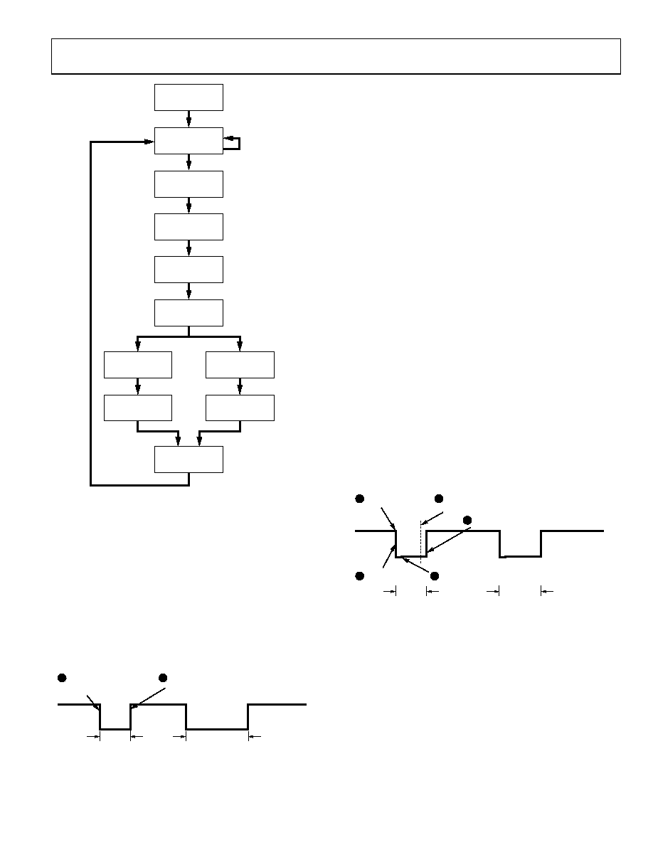
Figure 57. BSD Slave Node State Machine
BSD PERIOD
IN 0 STATE
BSD PERIOD
IN 1 STATE
LHSVAL0 LOADED
INTO LHSCAP HERE
2
MASTER DRIVES
BSD BUS LOW
1
SOFTWARE ASSERTS
BSD LOW HERE
3
SOFTWARE DEASSERTS
BSD HIGH HERE
5
LHSCMP = LHSVAL0
INTERRUPT GENERATED
HERE
4
07
47
4-
05
6
BSD DATA RECEPTION
To receive data, the LIN/BSD peripheral must first be con-
figured in BSD mode where LHSCON0[6] = 1. In this mode,
LHSCON0[8] should be set to ensure that the LHS break timer
section) generates an interrupt on the rising edge of the BSD bus.
The LHS break timer is cleared and starts counting on the falling
edge of the BSD bus; the timer is subsequently stopped and
generates an interrupt on the rising edge of the BSD bus. Given
that the LHS break timer is clocked by the low power 131 kHz
oscillator, the value in LHSVAL1 can be interpreted by user code
to determine if the received data bit is a BSD sync pulse, 0, or 1.
Figure 59. Master Read, Slave Transmit
WAKE-UP FROM BSD INTERFACE
The MCU core can be awakened from power-down via the BSD
physical interface. Before entering power-down mode, user code
should enable the start condition interrupt (LHSCON0[3]). When
this interrupt is enabled, a high-to-low transition on the LIN/BSD
pin generates an interrupt event and wakes up the MCU core.
BSD PERIOD
IN 0 STATE
BSD PERIOD
IN 1 STATE
LHSVAL1 CLEARED
AND STARTS COUNTING
ON THIS EDGE
1
LHSVAL1 STOPPED
AND GENERATES
INTERRUPT ON THIS EDGE
2
07
47
4-
05
5
Figure 58. Master Transmit, Slave Read
相关PDF资料 |
PDF描述 |
|---|---|
| ATSAM3X4EA-AU | IC MCU 2X128KB CORTEX-M3 144-QFP |
| AT91SAM7X128C-AU | IC MCU 32BIT 128KB FLASH 100LQFP |
| NC7WB66L8X | IC SWITCH DUAL SPST-NO 8MICROPAK |
| MC74HCT4051ADR2G | ANALOG MULTIPLEXERS/DEMU SOIC16 |
| VE-B4P-IX | CONVERTER MOD DC/DC 13.8V 75W |
相关代理商/技术参数 |
参数描述 |
|---|---|
| ADUC7036BCPZ-RL | 功能描述:IC SENSOR AUTO 96K FLASH 48LFCSP RoHS:是 类别:集成电路 (IC) >> 嵌入式 - 微控制器, 系列:MicroConverter® ADuC7xxx 标准包装:38 系列:Encore!® XP® 核心处理器:eZ8 芯体尺寸:8-位 速度:5MHz 连通性:IrDA,UART/USART 外围设备:欠压检测/复位,LED,POR,PWM,WDT 输入/输出数:16 程序存储器容量:4KB(4K x 8) 程序存储器类型:闪存 EEPROM 大小:- RAM 容量:1K x 8 电压 - 电源 (Vcc/Vdd):2.7 V ~ 3.6 V 数据转换器:- 振荡器型:内部 工作温度:-40°C ~ 105°C 封装/外壳:20-SOIC(0.295",7.50mm 宽) 包装:管件 其它名称:269-4116Z8F0413SH005EG-ND |
| ADUC7036CCPZ | 功能描述:IC MCU 96K FLASH DUAL 48LFCSP RoHS:是 类别:集成电路 (IC) >> 嵌入式 - 微控制器, 系列:MicroConverter® ADuC7xxx 标准包装:38 系列:Encore!® XP® 核心处理器:eZ8 芯体尺寸:8-位 速度:5MHz 连通性:IrDA,UART/USART 外围设备:欠压检测/复位,LED,POR,PWM,WDT 输入/输出数:16 程序存储器容量:4KB(4K x 8) 程序存储器类型:闪存 EEPROM 大小:- RAM 容量:1K x 8 电压 - 电源 (Vcc/Vdd):2.7 V ~ 3.6 V 数据转换器:- 振荡器型:内部 工作温度:-40°C ~ 105°C 封装/外壳:20-SOIC(0.295",7.50mm 宽) 包装:管件 其它名称:269-4116Z8F0413SH005EG-ND |
| ADUC7036CCPZ-RL | 功能描述:IC MCU 96K FLASH DUAL 48LFCSP RoHS:是 类别:集成电路 (IC) >> 嵌入式 - 微控制器, 系列:MicroConverter® ADuC7xxx 标准包装:38 系列:Encore!® XP® 核心处理器:eZ8 芯体尺寸:8-位 速度:5MHz 连通性:IrDA,UART/USART 外围设备:欠压检测/复位,LED,POR,PWM,WDT 输入/输出数:16 程序存储器容量:4KB(4K x 8) 程序存储器类型:闪存 EEPROM 大小:- RAM 容量:1K x 8 电压 - 电源 (Vcc/Vdd):2.7 V ~ 3.6 V 数据转换器:- 振荡器型:内部 工作温度:-40°C ~ 105°C 封装/外壳:20-SOIC(0.295",7.50mm 宽) 包装:管件 其它名称:269-4116Z8F0413SH005EG-ND |
| ADUC7036DCPZ | 功能描述:IC MCU 96K FLASH DUAL 48LFCSP RoHS:是 类别:集成电路 (IC) >> 嵌入式 - 微控制器, 系列:MicroConverter® ADuC7xxx 标准包装:38 系列:Encore!® XP® 核心处理器:eZ8 芯体尺寸:8-位 速度:5MHz 连通性:IrDA,UART/USART 外围设备:欠压检测/复位,LED,POR,PWM,WDT 输入/输出数:16 程序存储器容量:4KB(4K x 8) 程序存储器类型:闪存 EEPROM 大小:- RAM 容量:1K x 8 电压 - 电源 (Vcc/Vdd):2.7 V ~ 3.6 V 数据转换器:- 振荡器型:内部 工作温度:-40°C ~ 105°C 封装/外壳:20-SOIC(0.295",7.50mm 宽) 包装:管件 其它名称:269-4116Z8F0413SH005EG-ND |
| ADUC7036DCPZ-RL | 功能描述:IC MCU 96K FLASH DUAL 48LFCSP RoHS:是 类别:集成电路 (IC) >> 嵌入式 - 微控制器, 系列:MicroConverter® ADuC7xxx 标准包装:38 系列:Encore!® XP® 核心处理器:eZ8 芯体尺寸:8-位 速度:5MHz 连通性:IrDA,UART/USART 外围设备:欠压检测/复位,LED,POR,PWM,WDT 输入/输出数:16 程序存储器容量:4KB(4K x 8) 程序存储器类型:闪存 EEPROM 大小:- RAM 容量:1K x 8 电压 - 电源 (Vcc/Vdd):2.7 V ~ 3.6 V 数据转换器:- 振荡器型:内部 工作温度:-40°C ~ 105°C 封装/外壳:20-SOIC(0.295",7.50mm 宽) 包装:管件 其它名称:269-4116Z8F0413SH005EG-ND |
发布紧急采购,3分钟左右您将得到回复。