- 您现在的位置:买卖IC网 > PDF目录11199 > ADUC7036BCPZ (Analog Devices Inc)IC MCU FLASH 96K ANLGI/O 48LFCSP PDF资料下载
参数资料
| 型号: | ADUC7036BCPZ |
| 厂商: | Analog Devices Inc |
| 文件页数: | 31/132页 |
| 文件大小: | 0K |
| 描述: | IC MCU FLASH 96K ANLGI/O 48LFCSP |
| 产品培训模块: | Process Control |
| 标准包装: | 1 |
| 系列: | MicroConverter® ADuC7xxx |
| 核心处理器: | ARM7 |
| 芯体尺寸: | 16/32-位 |
| 速度: | 20.48MHz |
| 连通性: | LIN,SPI,UART/USART |
| 外围设备: | PSM,温度传感器,WDT |
| 输入/输出数: | 9 |
| 程序存储器容量: | 96KB(48K x 16) |
| 程序存储器类型: | 闪存 |
| RAM 容量: | 1.5K x 32 |
| 电压 - 电源 (Vcc/Vdd): | 3.5 V ~ 18 V |
| 数据转换器: | A/D 2x16b |
| 振荡器型: | 内部 |
| 工作温度: | -40°C ~ 115°C |
| 封装/外壳: | 48-VFQFN 裸露焊盘,CSP |
| 包装: | 托盘 |
第1页第2页第3页第4页第5页第6页第7页第8页第9页第10页第11页第12页第13页第14页第15页第16页第17页第18页第19页第20页第21页第22页第23页第24页第25页第26页第27页第28页第29页第30页当前第31页第32页第33页第34页第35页第36页第37页第38页第39页第40页第41页第42页第43页第44页第45页第46页第47页第48页第49页第50页第51页第52页第53页第54页第55页第56页第57页第58页第59页第60页第61页第62页第63页第64页第65页第66页第67页第68页第69页第70页第71页第72页第73页第74页第75页第76页第77页第78页第79页第80页第81页第82页第83页第84页第85页第86页第87页第88页第89页第90页第91页第92页第93页第94页第95页第96页第97页第98页第99页第100页第101页第102页第103页第104页第105页第106页第107页第108页第109页第110页第111页第112页第113页第114页第115页第116页第117页第118页第119页第120页第121页第122页第123页第124页第125页第126页第127页第128页第129页第130页第131页第132页
ADuC7036
Rev. C | Page 126 of 132
BSD COMMUNICATION FRAME
To transfer data between a master and slave, or vice versa, the
construction of a BSD frame is required. A BSD frame contains
seven key components: pause/sync, a direction (DIR) bit, the
slave address, the register address, data, parity bits (P1 and P2),
and the acknowledge bit from the slave.
If the master is transmitting data, all bits except the acknowledge
bit are transmitted by the master.
If the master is requesting data from the slave, the master transmits
the pause/sync, direction bit, slave address, register address, and
P1. The slave then transmits the data bytes, the P2 bit, and the
acknowledge bit in the following sequence:
1.
Pause: ≥ three synchronization pulses
2.
DIR: signifies the direction of data transfer
DIR = 0 if master sends request
DIR = 1 if slave sends request
3.
Slave address
4.
Register address: defines register to be read or written
5.
Bit 3 is set to write and cleared to read
6.
Data: 8-bit read only receive register
7.
P1 and P2
P1 = 0 if even number of 1s in eight previous bits
P1 = 1 if odd number of 1s in eight previous bits
P2 = 0 if even number of 1s in data-word
P2 = 1 if odd number of 1s in data-word
8.
Acknowledge bit
ACK = 0 if transmission is successful
The acknowledge bit is always transmitted by the slave to
indicate whether the information was received or transmitted.
Table 96. BSD Protocol Description
Pause
DIR
Slave
Address
Register
Address
P1
Data
P2
ACK
3 bits
1 bit
3 bits
4 bits
1 bit
8 bits
1 bit
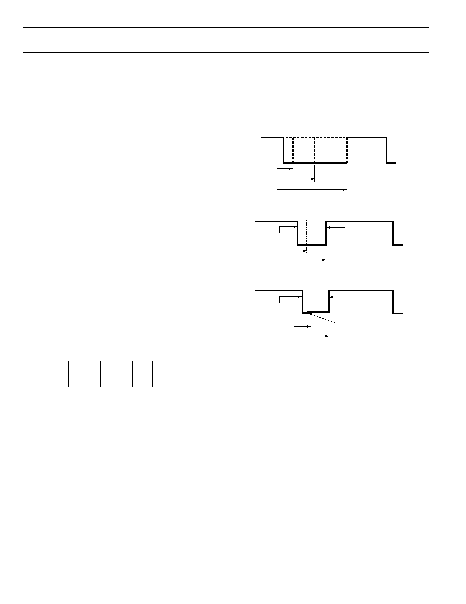
BSD Example Pulse Widths
An example of the different pulse widths is shown in Figure 54.
For each bit, the period for which the bus is held low defines
what type of bit it is. If the bit is a sync bit, the pulse is held low
for one bit. If the bit is 0, the pulse is held low for three bits. If
the bit is 1, the pulse is held low for six bits.
If the master is transmitting data, the signal is held low for the
duration of the signal by the master. An example of a master
transmitting a 0 is shown in Figure 55. If the slave is
transmitting data, the master pulls the bus low to begin
communication. The slave must pull the bus low before tSYNC
elapses and then hold the bus low until either t0 or t1 has elapsed,
after which time the bus is released by the slave. An example of a
slave transmitting a 0 is shown in Figure 56.
tSYNC
t0
t1
07
47
4-
05
1
Figure 54. BSD Bit Transmission
BUS PULLED LOW
BY MASTER
tSYNC
BUS RELEASED BY
MASTER AFTER
t0
07
47
4-
05
2
Figure 55. BSD Master Transmitting a 0
BUS PULLED LOW
BY MASTER
BUS RELEASED BY
SLAVE AFTER
t0
BUS HELD LOW
BY SLAVE
RELEASED BY
MASTER
tSYNC
t0
07
47
4-
05
3
Figure 56. BSD Slave Transmitting a 0
Typical BSD Program Flow
Because BSD is a PWM communication protocol controlled by
software, the user must construct the required data from each bit.
For example, in constructing the slave address, the slave node
receives the three bits and the user constructs the relevant address.
When BSD communication is initiated by the master, data is
transmitted and received by the slave node. A flowchart showing
this process is shown in Figure 57.
相关PDF资料 |
PDF描述 |
|---|---|
| ATSAM3X4EA-AU | IC MCU 2X128KB CORTEX-M3 144-QFP |
| AT91SAM7X128C-AU | IC MCU 32BIT 128KB FLASH 100LQFP |
| NC7WB66L8X | IC SWITCH DUAL SPST-NO 8MICROPAK |
| MC74HCT4051ADR2G | ANALOG MULTIPLEXERS/DEMU SOIC16 |
| VE-B4P-IX | CONVERTER MOD DC/DC 13.8V 75W |
相关代理商/技术参数 |
参数描述 |
|---|---|
| ADUC7036BCPZ-RL | 功能描述:IC SENSOR AUTO 96K FLASH 48LFCSP RoHS:是 类别:集成电路 (IC) >> 嵌入式 - 微控制器, 系列:MicroConverter® ADuC7xxx 标准包装:38 系列:Encore!® XP® 核心处理器:eZ8 芯体尺寸:8-位 速度:5MHz 连通性:IrDA,UART/USART 外围设备:欠压检测/复位,LED,POR,PWM,WDT 输入/输出数:16 程序存储器容量:4KB(4K x 8) 程序存储器类型:闪存 EEPROM 大小:- RAM 容量:1K x 8 电压 - 电源 (Vcc/Vdd):2.7 V ~ 3.6 V 数据转换器:- 振荡器型:内部 工作温度:-40°C ~ 105°C 封装/外壳:20-SOIC(0.295",7.50mm 宽) 包装:管件 其它名称:269-4116Z8F0413SH005EG-ND |
| ADUC7036CCPZ | 功能描述:IC MCU 96K FLASH DUAL 48LFCSP RoHS:是 类别:集成电路 (IC) >> 嵌入式 - 微控制器, 系列:MicroConverter® ADuC7xxx 标准包装:38 系列:Encore!® XP® 核心处理器:eZ8 芯体尺寸:8-位 速度:5MHz 连通性:IrDA,UART/USART 外围设备:欠压检测/复位,LED,POR,PWM,WDT 输入/输出数:16 程序存储器容量:4KB(4K x 8) 程序存储器类型:闪存 EEPROM 大小:- RAM 容量:1K x 8 电压 - 电源 (Vcc/Vdd):2.7 V ~ 3.6 V 数据转换器:- 振荡器型:内部 工作温度:-40°C ~ 105°C 封装/外壳:20-SOIC(0.295",7.50mm 宽) 包装:管件 其它名称:269-4116Z8F0413SH005EG-ND |
| ADUC7036CCPZ-RL | 功能描述:IC MCU 96K FLASH DUAL 48LFCSP RoHS:是 类别:集成电路 (IC) >> 嵌入式 - 微控制器, 系列:MicroConverter® ADuC7xxx 标准包装:38 系列:Encore!® XP® 核心处理器:eZ8 芯体尺寸:8-位 速度:5MHz 连通性:IrDA,UART/USART 外围设备:欠压检测/复位,LED,POR,PWM,WDT 输入/输出数:16 程序存储器容量:4KB(4K x 8) 程序存储器类型:闪存 EEPROM 大小:- RAM 容量:1K x 8 电压 - 电源 (Vcc/Vdd):2.7 V ~ 3.6 V 数据转换器:- 振荡器型:内部 工作温度:-40°C ~ 105°C 封装/外壳:20-SOIC(0.295",7.50mm 宽) 包装:管件 其它名称:269-4116Z8F0413SH005EG-ND |
| ADUC7036DCPZ | 功能描述:IC MCU 96K FLASH DUAL 48LFCSP RoHS:是 类别:集成电路 (IC) >> 嵌入式 - 微控制器, 系列:MicroConverter® ADuC7xxx 标准包装:38 系列:Encore!® XP® 核心处理器:eZ8 芯体尺寸:8-位 速度:5MHz 连通性:IrDA,UART/USART 外围设备:欠压检测/复位,LED,POR,PWM,WDT 输入/输出数:16 程序存储器容量:4KB(4K x 8) 程序存储器类型:闪存 EEPROM 大小:- RAM 容量:1K x 8 电压 - 电源 (Vcc/Vdd):2.7 V ~ 3.6 V 数据转换器:- 振荡器型:内部 工作温度:-40°C ~ 105°C 封装/外壳:20-SOIC(0.295",7.50mm 宽) 包装:管件 其它名称:269-4116Z8F0413SH005EG-ND |
| ADUC7036DCPZ-RL | 功能描述:IC MCU 96K FLASH DUAL 48LFCSP RoHS:是 类别:集成电路 (IC) >> 嵌入式 - 微控制器, 系列:MicroConverter® ADuC7xxx 标准包装:38 系列:Encore!® XP® 核心处理器:eZ8 芯体尺寸:8-位 速度:5MHz 连通性:IrDA,UART/USART 外围设备:欠压检测/复位,LED,POR,PWM,WDT 输入/输出数:16 程序存储器容量:4KB(4K x 8) 程序存储器类型:闪存 EEPROM 大小:- RAM 容量:1K x 8 电压 - 电源 (Vcc/Vdd):2.7 V ~ 3.6 V 数据转换器:- 振荡器型:内部 工作温度:-40°C ~ 105°C 封装/外壳:20-SOIC(0.295",7.50mm 宽) 包装:管件 其它名称:269-4116Z8F0413SH005EG-ND |
发布紧急采购,3分钟左右您将得到回复。