- 您现在的位置:买卖IC网 > PDF目录11199 > ADUC7036BCPZ (Analog Devices Inc)IC MCU FLASH 96K ANLGI/O 48LFCSP PDF资料下载
参数资料
| 型号: | ADUC7036BCPZ |
| 厂商: | Analog Devices Inc |
| 文件页数: | 85/132页 |
| 文件大小: | 0K |
| 描述: | IC MCU FLASH 96K ANLGI/O 48LFCSP |
| 产品培训模块: | Process Control |
| 标准包装: | 1 |
| 系列: | MicroConverter® ADuC7xxx |
| 核心处理器: | ARM7 |
| 芯体尺寸: | 16/32-位 |
| 速度: | 20.48MHz |
| 连通性: | LIN,SPI,UART/USART |
| 外围设备: | PSM,温度传感器,WDT |
| 输入/输出数: | 9 |
| 程序存储器容量: | 96KB(48K x 16) |
| 程序存储器类型: | 闪存 |
| RAM 容量: | 1.5K x 32 |
| 电压 - 电源 (Vcc/Vdd): | 3.5 V ~ 18 V |
| 数据转换器: | A/D 2x16b |
| 振荡器型: | 内部 |
| 工作温度: | -40°C ~ 115°C |
| 封装/外壳: | 48-VFQFN 裸露焊盘,CSP |
| 包装: | 托盘 |
第1页第2页第3页第4页第5页第6页第7页第8页第9页第10页第11页第12页第13页第14页第15页第16页第17页第18页第19页第20页第21页第22页第23页第24页第25页第26页第27页第28页第29页第30页第31页第32页第33页第34页第35页第36页第37页第38页第39页第40页第41页第42页第43页第44页第45页第46页第47页第48页第49页第50页第51页第52页第53页第54页第55页第56页第57页第58页第59页第60页第61页第62页第63页第64页第65页第66页第67页第68页第69页第70页第71页第72页第73页第74页第75页第76页第77页第78页第79页第80页第81页第82页第83页第84页当前第85页第86页第87页第88页第89页第90页第91页第92页第93页第94页第95页第96页第97页第98页第99页第100页第101页第102页第103页第104页第105页第106页第107页第108页第109页第110页第111页第112页第113页第114页第115页第116页第117页第118页第119页第120页第121页第122页第123页第124页第125页第126页第127页第128页第129页第130页第131页第132页
ADuC7036
Rev. C | Page 56 of 132
ADC COMPARATOR AND ACCUMULATOR
The incorporation of comparator logic on the I-ADC allows the
I-ADC result to generate an interrupt after a predefined number of
conversions has elapsed or a programmable threshold value has
been exceeded.
Every I-ADC result can be compared with a preset threshold
level (ADC0TH) that is set via ADCCFG[4:3]. In this case, an
MCU interrupt is generated if the absolute (sign independent)
value of the ADC result is greater than the preprogrammed
comparator threshold level. Alternatively, as an extended
function of the comparator, user code can configure a threshold
counter (ADC0THV) to monitor the number of I-ADC results
that have occurred above or below the preset threshold level. In
this case, an ADC interrupt is generated when the threshold
counter reaches a preset value that is set via ADC0TCL.
By also incorporating a 32-bit accumulator (ADC0ACC) function
that can be configured via ADCCFG[6:5], the I-ADC can add or
subtract multiple I-ADC sample results. User code can read the
accumulated value directly (ADC0ACC) without any further
software processing.
ADC SINC3 DIGITAL FILTER RESPONSE
The overall frequency response on all ADuC7036 ADCs is
dominated by the low-pass filter response of the on-chip Sinc3
digital filters. The Sinc3 filters are used to decimate the ADC
Σ-Δ modulator output data bit stream to generate a valid 16-bit
data result. The digital filter response is identical for all ADCs
and is configured via the 16-bit ADC filter register (ADCFLT).
This register determines the overall throughput rate of the ADCs.
The noise resolution of the ADCs is determined by the pro-
grammed ADC throughput rate. In the case of the current
channel ADC, the noise resolution is determined by throughput
rate and selected gain.
The overall frequency response and the ADC throughput is
dominated by the configuration of the Sinc3 filter decimation
factor (SF) bits (ADCFLT[6:0]) and the averaging factor (AF)
bits (ADCFLT[13:8]). Due to limitations on the digital filter
internal data path, there are some limitations on the allowable
combinations of SF and AF that can be used to generate a required
ADC output rate. This restriction limits the minimum ADC
update to 4 Hz in normal power mode and to 1 Hz in low power
mode. The calculation of the ADC throughput rate is detailed
in the ADCFLT bit designations table (see Table 39), and the
restrictions on allowable combinations of AF and SF values are
outlined in Table 41.
By default, setting ADCFLT = 0x0007 configures the ADCs for
a throughput of 1 kHz with all other filtering options (chop,
running average, averaging factor, and Sinc3 modify) disabled.
A typical filter response based on this default configuration is
shown in Figure 22.
–100
0
–10
–20
–30
–40
–50
–60
–70
–80
–90
0
500 1000 1500 2000 2500 3000 3500 4000 4500 5000
AT
T
E
NUA
T
IO
N
(
d
B)
FREQUENCY (kHz)
07
47
4-
02
1
Figure 22. Typical Digital Filter Response at fADC = 1 kHz
(ADCFLT = 0x0007)
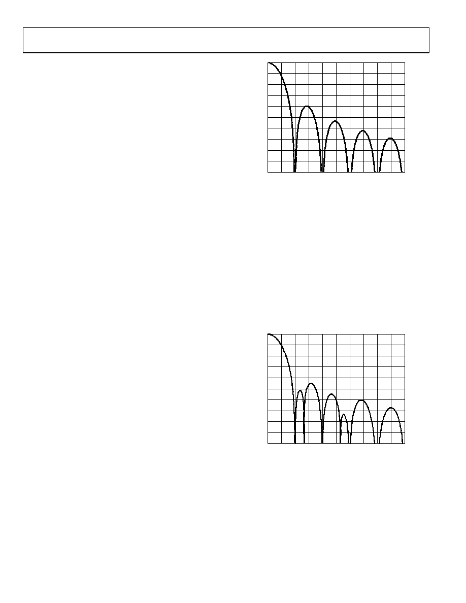
In addition, a Sinc3 modify bit (ADCFLT[7]) is available in the
ADCFLT register. This bit is set by user code and modifies the
standard Sinc3 frequency response to increase the filter stop-
band rejection by approximately 5 dB. This is achieved by
inserting a second notch at the location determined by
fNOTCH2 = 1.333 × fNOTCH
where fNOTCH is the location of the first notch in the response.
There is a slight increase in ADC noise if the Sinc3 modify bit is
active. Figure 23 shows the modified 1 kHz filter response when
the Sinc3 modify bit is active. The new notch is clearly visible at
1.33 kHz, as is the improvement in stop-band rejection when
compared with the standard 1 kHz response.
AT
T
E
N
UAT
IO
N
(
d
B
)
FREQUENCY (kHz)
–100
0
–10
–20
–30
–40
–50
–60
–70
–80
–90
0
0.5
1.5
2.5
3.5
4.0
4.5
3.0
2.0
1.0
5.0
07
47
4-
02
2
Figure 23. Modified Sinc3 Digital Filter Response at fADC = 1 kHz
(ADCFLT = 0x0087)
相关PDF资料 |
PDF描述 |
|---|---|
| ATSAM3X4EA-AU | IC MCU 2X128KB CORTEX-M3 144-QFP |
| AT91SAM7X128C-AU | IC MCU 32BIT 128KB FLASH 100LQFP |
| NC7WB66L8X | IC SWITCH DUAL SPST-NO 8MICROPAK |
| MC74HCT4051ADR2G | ANALOG MULTIPLEXERS/DEMU SOIC16 |
| VE-B4P-IX | CONVERTER MOD DC/DC 13.8V 75W |
相关代理商/技术参数 |
参数描述 |
|---|---|
| ADUC7036BCPZ-RL | 功能描述:IC SENSOR AUTO 96K FLASH 48LFCSP RoHS:是 类别:集成电路 (IC) >> 嵌入式 - 微控制器, 系列:MicroConverter® ADuC7xxx 标准包装:38 系列:Encore!® XP® 核心处理器:eZ8 芯体尺寸:8-位 速度:5MHz 连通性:IrDA,UART/USART 外围设备:欠压检测/复位,LED,POR,PWM,WDT 输入/输出数:16 程序存储器容量:4KB(4K x 8) 程序存储器类型:闪存 EEPROM 大小:- RAM 容量:1K x 8 电压 - 电源 (Vcc/Vdd):2.7 V ~ 3.6 V 数据转换器:- 振荡器型:内部 工作温度:-40°C ~ 105°C 封装/外壳:20-SOIC(0.295",7.50mm 宽) 包装:管件 其它名称:269-4116Z8F0413SH005EG-ND |
| ADUC7036CCPZ | 功能描述:IC MCU 96K FLASH DUAL 48LFCSP RoHS:是 类别:集成电路 (IC) >> 嵌入式 - 微控制器, 系列:MicroConverter® ADuC7xxx 标准包装:38 系列:Encore!® XP® 核心处理器:eZ8 芯体尺寸:8-位 速度:5MHz 连通性:IrDA,UART/USART 外围设备:欠压检测/复位,LED,POR,PWM,WDT 输入/输出数:16 程序存储器容量:4KB(4K x 8) 程序存储器类型:闪存 EEPROM 大小:- RAM 容量:1K x 8 电压 - 电源 (Vcc/Vdd):2.7 V ~ 3.6 V 数据转换器:- 振荡器型:内部 工作温度:-40°C ~ 105°C 封装/外壳:20-SOIC(0.295",7.50mm 宽) 包装:管件 其它名称:269-4116Z8F0413SH005EG-ND |
| ADUC7036CCPZ-RL | 功能描述:IC MCU 96K FLASH DUAL 48LFCSP RoHS:是 类别:集成电路 (IC) >> 嵌入式 - 微控制器, 系列:MicroConverter® ADuC7xxx 标准包装:38 系列:Encore!® XP® 核心处理器:eZ8 芯体尺寸:8-位 速度:5MHz 连通性:IrDA,UART/USART 外围设备:欠压检测/复位,LED,POR,PWM,WDT 输入/输出数:16 程序存储器容量:4KB(4K x 8) 程序存储器类型:闪存 EEPROM 大小:- RAM 容量:1K x 8 电压 - 电源 (Vcc/Vdd):2.7 V ~ 3.6 V 数据转换器:- 振荡器型:内部 工作温度:-40°C ~ 105°C 封装/外壳:20-SOIC(0.295",7.50mm 宽) 包装:管件 其它名称:269-4116Z8F0413SH005EG-ND |
| ADUC7036DCPZ | 功能描述:IC MCU 96K FLASH DUAL 48LFCSP RoHS:是 类别:集成电路 (IC) >> 嵌入式 - 微控制器, 系列:MicroConverter® ADuC7xxx 标准包装:38 系列:Encore!® XP® 核心处理器:eZ8 芯体尺寸:8-位 速度:5MHz 连通性:IrDA,UART/USART 外围设备:欠压检测/复位,LED,POR,PWM,WDT 输入/输出数:16 程序存储器容量:4KB(4K x 8) 程序存储器类型:闪存 EEPROM 大小:- RAM 容量:1K x 8 电压 - 电源 (Vcc/Vdd):2.7 V ~ 3.6 V 数据转换器:- 振荡器型:内部 工作温度:-40°C ~ 105°C 封装/外壳:20-SOIC(0.295",7.50mm 宽) 包装:管件 其它名称:269-4116Z8F0413SH005EG-ND |
| ADUC7036DCPZ-RL | 功能描述:IC MCU 96K FLASH DUAL 48LFCSP RoHS:是 类别:集成电路 (IC) >> 嵌入式 - 微控制器, 系列:MicroConverter® ADuC7xxx 标准包装:38 系列:Encore!® XP® 核心处理器:eZ8 芯体尺寸:8-位 速度:5MHz 连通性:IrDA,UART/USART 外围设备:欠压检测/复位,LED,POR,PWM,WDT 输入/输出数:16 程序存储器容量:4KB(4K x 8) 程序存储器类型:闪存 EEPROM 大小:- RAM 容量:1K x 8 电压 - 电源 (Vcc/Vdd):2.7 V ~ 3.6 V 数据转换器:- 振荡器型:内部 工作温度:-40°C ~ 105°C 封装/外壳:20-SOIC(0.295",7.50mm 宽) 包装:管件 其它名称:269-4116Z8F0413SH005EG-ND |
发布紧急采购,3分钟左右您将得到回复。