- 您现在的位置:买卖IC网 > PDF目录11199 > ADUC7036BCPZ (Analog Devices Inc)IC MCU FLASH 96K ANLGI/O 48LFCSP PDF资料下载
参数资料
| 型号: | ADUC7036BCPZ |
| 厂商: | Analog Devices Inc |
| 文件页数: | 48/132页 |
| 文件大小: | 0K |
| 描述: | IC MCU FLASH 96K ANLGI/O 48LFCSP |
| 产品培训模块: | Process Control |
| 标准包装: | 1 |
| 系列: | MicroConverter® ADuC7xxx |
| 核心处理器: | ARM7 |
| 芯体尺寸: | 16/32-位 |
| 速度: | 20.48MHz |
| 连通性: | LIN,SPI,UART/USART |
| 外围设备: | PSM,温度传感器,WDT |
| 输入/输出数: | 9 |
| 程序存储器容量: | 96KB(48K x 16) |
| 程序存储器类型: | 闪存 |
| RAM 容量: | 1.5K x 32 |
| 电压 - 电源 (Vcc/Vdd): | 3.5 V ~ 18 V |
| 数据转换器: | A/D 2x16b |
| 振荡器型: | 内部 |
| 工作温度: | -40°C ~ 115°C |
| 封装/外壳: | 48-VFQFN 裸露焊盘,CSP |
| 包装: | 托盘 |
第1页第2页第3页第4页第5页第6页第7页第8页第9页第10页第11页第12页第13页第14页第15页第16页第17页第18页第19页第20页第21页第22页第23页第24页第25页第26页第27页第28页第29页第30页第31页第32页第33页第34页第35页第36页第37页第38页第39页第40页第41页第42页第43页第44页第45页第46页第47页当前第48页第49页第50页第51页第52页第53页第54页第55页第56页第57页第58页第59页第60页第61页第62页第63页第64页第65页第66页第67页第68页第69页第70页第71页第72页第73页第74页第75页第76页第77页第78页第79页第80页第81页第82页第83页第84页第85页第86页第87页第88页第89页第90页第91页第92页第93页第94页第95页第96页第97页第98页第99页第100页第101页第102页第103页第104页第105页第106页第107页第108页第109页第110页第111页第112页第113页第114页第115页第116页第117页第118页第119页第120页第121页第122页第123页第124页第125页第126页第127页第128页第129页第130页第131页第132页
ADuC7036
Rev. C | Page 22 of 132
The minimum latency for FIQ or IRQ interrupts is five cycles.
This consists of the shortest time the request can take through
the synchronizer plus the time to enter the exception mode.
Note that the ARM7TDMI initially (first instruction) runs in
ARM (32-bit) mode when an exception occurs. The user can
immediately switch from ARM mode to Thumb mode if
required, for example, when executing interrupt service routines.
MEMORY ORGANIZATION
The ARM7 MCU core, which has a von Neumann-based
architecture, sees memory as a linear array of 232 byte locations.
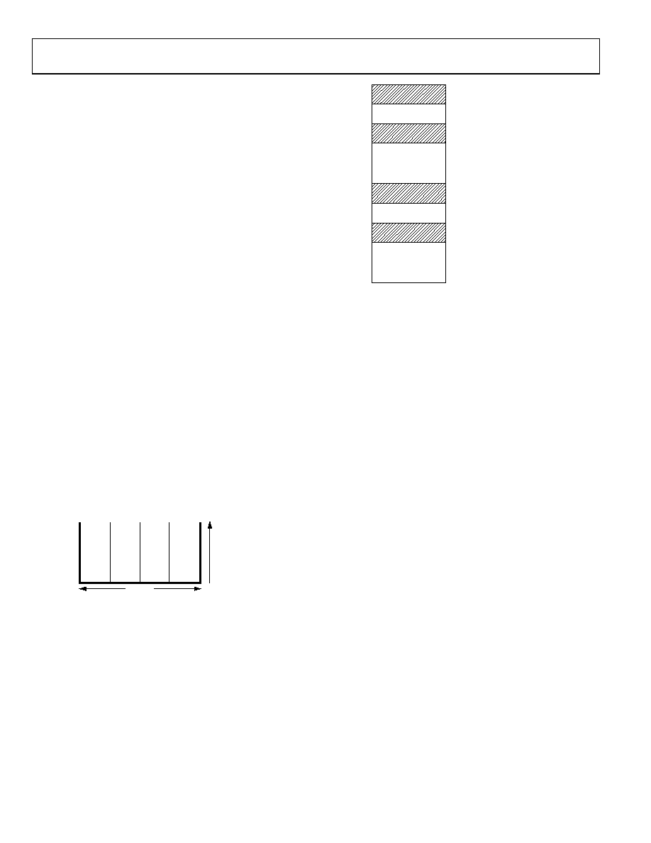
As shown in Figure 13, the ADuC7036 maps this into four
distinct user areas: a memory area that can be remapped, an
SRAM area, a Flash/EE area, and a memory mapped register
(MMR) area.
The first 94 kB of this memory space is used as an area into
which the on-chip Flash/EE or SRAM can be remapped.
The ADuC7036 features a second 4 kB area at the top of
the memory map used to locate the MMRs, through which
all on-chip peripherals are configured and monitored.
The ADuC7036 features an SRAM size of 6 kB.
The ADuC7036 features 96 kB of on-chip Flash/EE memory,
94 kB of which are available to the user and 2 kB of which
are reserved for the on-chip kernel.
Any access, either a read or a write, to an area not defined in the
memory map results in a data abort exception.
Memory Format
The ADuC7036 memory organization is configured in little
endian format: the least significant byte is located in the lowest
byte address and the most significant byte in the highest byte
address.
BIT 31
BYTE 2
A
6
2
.
BYTE 3
B
7
3
.
BYTE 1
9
5
1
.
BYTE 0
8
4
0
.
BIT 0
32 BITS
0xFFFFFFFF
0x00000004
0x00000000
0
747
4-
0
12
Figure 12. Little Endian Format
0x00417FF
0x00040000
0xFFFF0FFF
0xFFFF0000
MMRs
0x00097FFF
0x00080000
FLASH/EE
SRAM
0x0017FFF
0x00000000
REMAPPABLE MEMORY SPACE
(FLASH/EE OR SRAM)
RESERVED
0
74
-01
3
Figure 13. Memory Map
SRAM
The ADuC7036 features 6 kB of SRAM, organized as
1536 × 32 bits, that is, 1536 words located at 0x00040000.
The RAM space can be used as data memory and also as a volatile
program space.
ARM code can run directly from SRAM at full clock speed
because the SRAM array is configured as a 32-bit-wide memory
array. SRAM is readable/writeable in 8-, 16-, and 32-bit segments.
Remap
The ARM exception vectors are situated at the bottom of the
memory array, from Address 0x00000000 to Address 0x00000020.
By default, after a reset, the Flash/EE memory is logically
mapped to Address 0x00000000.
It is possible to logically remap the SRAM to Address 0x00000000.
This is accomplished by setting Bit 0 of the SYSMAP0 MMR
located at 0xFFFF0220. To revert Flash/EE to 0x00000000, Bit 0
of SYSMAP0 is cleared.
It may be desirable to remap RAM to 0x00000000 to optimize the
interrupt latency of the ADuC7036 because code can run in full
32-bit ARM mode and at maximum core speed. It should be noted
that when an exception occurs, the core defaults to ARM mode.
相关PDF资料 |
PDF描述 |
|---|---|
| ATSAM3X4EA-AU | IC MCU 2X128KB CORTEX-M3 144-QFP |
| AT91SAM7X128C-AU | IC MCU 32BIT 128KB FLASH 100LQFP |
| NC7WB66L8X | IC SWITCH DUAL SPST-NO 8MICROPAK |
| MC74HCT4051ADR2G | ANALOG MULTIPLEXERS/DEMU SOIC16 |
| VE-B4P-IX | CONVERTER MOD DC/DC 13.8V 75W |
相关代理商/技术参数 |
参数描述 |
|---|---|
| ADUC7036BCPZ-RL | 功能描述:IC SENSOR AUTO 96K FLASH 48LFCSP RoHS:是 类别:集成电路 (IC) >> 嵌入式 - 微控制器, 系列:MicroConverter® ADuC7xxx 标准包装:38 系列:Encore!® XP® 核心处理器:eZ8 芯体尺寸:8-位 速度:5MHz 连通性:IrDA,UART/USART 外围设备:欠压检测/复位,LED,POR,PWM,WDT 输入/输出数:16 程序存储器容量:4KB(4K x 8) 程序存储器类型:闪存 EEPROM 大小:- RAM 容量:1K x 8 电压 - 电源 (Vcc/Vdd):2.7 V ~ 3.6 V 数据转换器:- 振荡器型:内部 工作温度:-40°C ~ 105°C 封装/外壳:20-SOIC(0.295",7.50mm 宽) 包装:管件 其它名称:269-4116Z8F0413SH005EG-ND |
| ADUC7036CCPZ | 功能描述:IC MCU 96K FLASH DUAL 48LFCSP RoHS:是 类别:集成电路 (IC) >> 嵌入式 - 微控制器, 系列:MicroConverter® ADuC7xxx 标准包装:38 系列:Encore!® XP® 核心处理器:eZ8 芯体尺寸:8-位 速度:5MHz 连通性:IrDA,UART/USART 外围设备:欠压检测/复位,LED,POR,PWM,WDT 输入/输出数:16 程序存储器容量:4KB(4K x 8) 程序存储器类型:闪存 EEPROM 大小:- RAM 容量:1K x 8 电压 - 电源 (Vcc/Vdd):2.7 V ~ 3.6 V 数据转换器:- 振荡器型:内部 工作温度:-40°C ~ 105°C 封装/外壳:20-SOIC(0.295",7.50mm 宽) 包装:管件 其它名称:269-4116Z8F0413SH005EG-ND |
| ADUC7036CCPZ-RL | 功能描述:IC MCU 96K FLASH DUAL 48LFCSP RoHS:是 类别:集成电路 (IC) >> 嵌入式 - 微控制器, 系列:MicroConverter® ADuC7xxx 标准包装:38 系列:Encore!® XP® 核心处理器:eZ8 芯体尺寸:8-位 速度:5MHz 连通性:IrDA,UART/USART 外围设备:欠压检测/复位,LED,POR,PWM,WDT 输入/输出数:16 程序存储器容量:4KB(4K x 8) 程序存储器类型:闪存 EEPROM 大小:- RAM 容量:1K x 8 电压 - 电源 (Vcc/Vdd):2.7 V ~ 3.6 V 数据转换器:- 振荡器型:内部 工作温度:-40°C ~ 105°C 封装/外壳:20-SOIC(0.295",7.50mm 宽) 包装:管件 其它名称:269-4116Z8F0413SH005EG-ND |
| ADUC7036DCPZ | 功能描述:IC MCU 96K FLASH DUAL 48LFCSP RoHS:是 类别:集成电路 (IC) >> 嵌入式 - 微控制器, 系列:MicroConverter® ADuC7xxx 标准包装:38 系列:Encore!® XP® 核心处理器:eZ8 芯体尺寸:8-位 速度:5MHz 连通性:IrDA,UART/USART 外围设备:欠压检测/复位,LED,POR,PWM,WDT 输入/输出数:16 程序存储器容量:4KB(4K x 8) 程序存储器类型:闪存 EEPROM 大小:- RAM 容量:1K x 8 电压 - 电源 (Vcc/Vdd):2.7 V ~ 3.6 V 数据转换器:- 振荡器型:内部 工作温度:-40°C ~ 105°C 封装/外壳:20-SOIC(0.295",7.50mm 宽) 包装:管件 其它名称:269-4116Z8F0413SH005EG-ND |
| ADUC7036DCPZ-RL | 功能描述:IC MCU 96K FLASH DUAL 48LFCSP RoHS:是 类别:集成电路 (IC) >> 嵌入式 - 微控制器, 系列:MicroConverter® ADuC7xxx 标准包装:38 系列:Encore!® XP® 核心处理器:eZ8 芯体尺寸:8-位 速度:5MHz 连通性:IrDA,UART/USART 外围设备:欠压检测/复位,LED,POR,PWM,WDT 输入/输出数:16 程序存储器容量:4KB(4K x 8) 程序存储器类型:闪存 EEPROM 大小:- RAM 容量:1K x 8 电压 - 电源 (Vcc/Vdd):2.7 V ~ 3.6 V 数据转换器:- 振荡器型:内部 工作温度:-40°C ~ 105°C 封装/外壳:20-SOIC(0.295",7.50mm 宽) 包装:管件 其它名称:269-4116Z8F0413SH005EG-ND |
发布紧急采购,3分钟左右您将得到回复。