- 您现在的位置:买卖IC网 > PDF目录11203 > ADUC7128BSTZ126-RL (Analog Devices Inc)IC DAS MCU ARM7 ADC/DDS 64-LQFP PDF资料下载
参数资料
| 型号: | ADUC7128BSTZ126-RL |
| 厂商: | Analog Devices Inc |
| 文件页数: | 20/92页 |
| 文件大小: | 0K |
| 描述: | IC DAS MCU ARM7 ADC/DDS 64-LQFP |
| 产品培训模块: | ARM7 Applications & Tools Intro to ARM7 Core & Microconverters Process Control Direct Digital Synthesis Tutorial Series (1 of 7): Introduction |
| 标准包装: | 1 |
| 系列: | MicroConverter® ADuC7xxx |
| 核心处理器: | ARM7 |
| 芯体尺寸: | 16/32-位 |
| 速度: | 41.78MHz |
| 连通性: | I²C,SPI,UART/USART |
| 外围设备: | PLA,POR,PWM,PSM,温度传感器,WDT |
| 输入/输出数: | 28 |
| 程序存储器容量: | 126KB(63K x 16) |
| 程序存储器类型: | 闪存 |
| RAM 容量: | 8K x 8 |
| 电压 - 电源 (Vcc/Vdd): | 3 V ~ 3.6 V |
| 数据转换器: | A/D 10x12b; D/A 1x10b |
| 振荡器型: | 内部 |
| 工作温度: | -40°C ~ 125°C |
| 封装/外壳: | 64-LQFP |
| 包装: | 标准包装 |
| 配用: | EVAL-ADUC7128QSPZ-ND - KIT DEV FOR ADUC7128 |
| 其它名称: | ADUC7128BSTZ126-RLDKR |
第1页第2页第3页第4页第5页第6页第7页第8页第9页第10页第11页第12页第13页第14页第15页第16页第17页第18页第19页当前第20页第21页第22页第23页第24页第25页第26页第27页第28页第29页第30页第31页第32页第33页第34页第35页第36页第37页第38页第39页第40页第41页第42页第43页第44页第45页第46页第47页第48页第49页第50页第51页第52页第53页第54页第55页第56页第57页第58页第59页第60页第61页第62页第63页第64页第65页第66页第67页第68页第69页第70页第71页第72页第73页第74页第75页第76页第77页第78页第79页第80页第81页第82页第83页第84页第85页第86页第87页第88页第89页第90页第91页第92页
ADuC7128/ADuC7129
Rev. 0 | Page 27 of 92
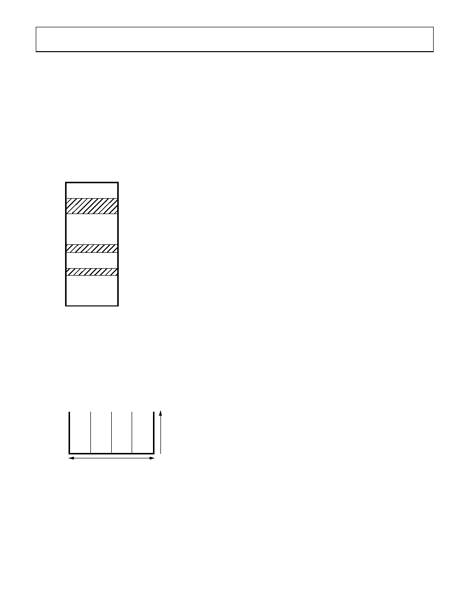
MEMORY ORGANIZATION
The ADuC7128/ADuC7129 incorporate three separate blocks
of memory: 8 kB of SRAM and two 64 kB of on-chip Flash/EE
memory. There are 126 kB of on-chip Flash/EE memory available
to the user, and the remaining 2 kB are reserved for the factory-
configured boot page. These two blocks are mapped as shown
in Figure 29.
Note that by default, after a reset, the Flash/EE memory is
mirrored at Address 0x00000000. It is possible to remap the
SRAM at Address 0x00000000 by clearing Bit 0 of the REMAP
MMR. This remap function is described in more detail in the
Flash/EE Memory section.
RESERVED
0x00080000
FLASH/EE
RESERVED
0x00041FFF
0x00040000
SRAM
0xFFFF0000
0xFFFFFFFF
MMRs
0x0001FFFF
0x00000000
0x0009F800
RESERVED
REMAPPABLE MEMORY SPACE
(FLASH/EE OR SRAM)
06
02
0-
0
25
Figure 29. Physical Memory Map
MEMORY ACCESS
The ARM7 core sees memory as a linear array of 232 byte
locations where the different blocks of memory are mapped as
outlined in Figure 29.
The ADuC7128/ADuC7129 memory organization is configured
in little endian format: the least significant byte is located in the
lowest byte address and the most significant byte in the highest
byte address.
BIT 31
BYTE 2
A
6
2
.
BYTE 3
B
7
3
.
BYTE 1
9
5
1
.
BYTE 0
8
4
0
.
BIT 0
32 BITS
0xFFFFFFFF
0x00000004
0x00000000
0
602
0-
0
26
Figure 30. Little Endian Format
FLASH/EE MEMORY
The 128 kB of Flash/EE is organized as two banks of 32 k ×
16 bits. In the first block, 31 k × 16 bits are user space and
1 k × 16 bits is reserved for the factory-configured boot
page. The page size of this Flash/EE memory is 512 bytes.
The second 64 kB block is organized in a similar manner. It is
arranged in 32 k × 16 bits. All of this is available as user space.
The 126 kB of Flash/EE is available to the user as code and
nonvolatile data memory. There is no distinction between data
and program as ARM code shares the same space. The real width
of the Flash/EE memory is 16 bits, meaning that in ARM mode
(32-bit instruction), two accesses to the Flash/EE are necessary
for each instruction fetch. Therefore, it is recommended that
Thumb mode be used when executing from Flash/EE memory
for optimum access speed. The maximum access speed for the
Flash/EE memory is 41.78 MHz in Thumb mode and 20.89 MHz
in full ARM mode (see the Execution Time from SRAM and
FLASH/EE section).
SRAM
The 8 kB of SRAM are available to the user, organized as 2 k ×
32 bits, that is, 2 k words. ARM code can run directly from SRAM
at 41.78 MHz, given that the SRAM array is configured as a
32-bit wide memory array (see the Execution Time from SRAM
and FLASH/EE section).
MEMORY MAPPED REGISTERS
The memory mapped register (MMR) space is mapped into the
upper two pages of the memory array and accessed by indirect
addressing through the ARM7 banked registers.
The MMR space provides an interface between the CPU and
all on-chip peripherals. All registers except the core registers
reside in the MMR area. All shaded locations shown in Figure 31
are unoccupied or reserved locations and should not be
a full MMR memory map.
The access time reading or writing a MMR depends on the
advanced microcontroller bus architecture (AMBA) bus used to
access the peripheral. The processor has two AMBA buses:
advanced high performance bus (AHB) used for system modules,
and advanced peripheral bus (APB) used for lower performance
peripherals. Access to the AHB is one cycle, and access to the
APB is two cycles. All peripherals on the ADuC7128/ADuC7129
are on the APB except the Flash/EE memory and the GPIOs.
相关PDF资料 |
PDF描述 |
|---|---|
| VI-BTJ-IX | CONVERTER MOD DC/DC 36V 75W |
| VI-BTJ-IW | CONVERTER MOD DC/DC 36V 100W |
| VI-BTH-IX | CONVERTER MOD DC/DC 52V 75W |
| AT91SAM7X256B-CU-999 | IC MCU ARM 256KB FLASH 100TFBGA |
| VI-BT4-IW | CONVERTER MOD DC/DC 48V 100W |
相关代理商/技术参数 |
参数描述 |
|---|---|
| ADUC7128BSTZ126-RL2 | 制造商:AD 制造商全称:Analog Devices 功能描述:Precision Analog Microcontroller ARM7TDMI MCU with 12-Bit ADC and DDS DAC |
| ADUC7129 | 制造商:AD 制造商全称:Analog Devices 功能描述:Precision Analog Microcontroller ARM7TDMI MCU with 12-Bit ADC and DDS DAC |
| ADUC7129BSTZ126 | 功能描述:IC DAS MCU ARM7 ADC/DDS 80-LQFP RoHS:是 类别:集成电路 (IC) >> 嵌入式 - 微控制器, 系列:MicroConverter® ADuC7xxx 标准包装:38 系列:Encore!® XP® 核心处理器:eZ8 芯体尺寸:8-位 速度:5MHz 连通性:IrDA,UART/USART 外围设备:欠压检测/复位,LED,POR,PWM,WDT 输入/输出数:16 程序存储器容量:4KB(4K x 8) 程序存储器类型:闪存 EEPROM 大小:- RAM 容量:1K x 8 电压 - 电源 (Vcc/Vdd):2.7 V ~ 3.6 V 数据转换器:- 振荡器型:内部 工作温度:-40°C ~ 105°C 封装/外壳:20-SOIC(0.295",7.50mm 宽) 包装:管件 其它名称:269-4116Z8F0413SH005EG-ND |
| ADUC7129BSTZ1262 | 制造商:AD 制造商全称:Analog Devices 功能描述:Precision Analog Microcontroller ARM7TDMI MCU with 12-Bit ADC and DDS DAC |
| ADUC7129BSTZ126-RL | 功能描述:IC DAS MCU ARM7 ADC/DDS 80-LQFP RoHS:是 类别:集成电路 (IC) >> 嵌入式 - 微控制器, 系列:MicroConverter® ADuC7xxx 产品培训模块:Graphics LCD System and PIC24 Interface Asynchronous Stimulus 标准包装:27 系列:PIC® 24H 核心处理器:PIC 芯体尺寸:16-位 速度:40 MIP 连通性:I²C,SPI,UART/USART 外围设备:欠压检测/复位,POR,PWM,WDT 输入/输出数:21 程序存储器容量:12KB(4K x 24) 程序存储器类型:闪存 EEPROM 大小:- RAM 容量:1K x 8 电压 - 电源 (Vcc/Vdd):3 V ~ 3.6 V 数据转换器:A/D 10x10b/12b 振荡器型:内部 工作温度:-40°C ~ 85°C 封装/外壳:28-SOIC(0.295",7.50mm 宽) 包装:管件 产品目录页面:648 (CN2011-ZH PDF) 配用:AC164339-ND - MODULE SKT FOR PM3 28SOICDV164033-ND - KIT START EXPLORER 16 MPLAB ICD2 |
发布紧急采购,3分钟左右您将得到回复。