- 您现在的位置:买卖IC网 > PDF目录11203 > ADUC7128BSTZ126-RL (Analog Devices Inc)IC DAS MCU ARM7 ADC/DDS 64-LQFP PDF资料下载
参数资料
| 型号: | ADUC7128BSTZ126-RL |
| 厂商: | Analog Devices Inc |
| 文件页数: | 82/92页 |
| 文件大小: | 0K |
| 描述: | IC DAS MCU ARM7 ADC/DDS 64-LQFP |
| 产品培训模块: | ARM7 Applications & Tools Intro to ARM7 Core & Microconverters Process Control Direct Digital Synthesis Tutorial Series (1 of 7): Introduction |
| 标准包装: | 1 |
| 系列: | MicroConverter® ADuC7xxx |
| 核心处理器: | ARM7 |
| 芯体尺寸: | 16/32-位 |
| 速度: | 41.78MHz |
| 连通性: | I²C,SPI,UART/USART |
| 外围设备: | PLA,POR,PWM,PSM,温度传感器,WDT |
| 输入/输出数: | 28 |
| 程序存储器容量: | 126KB(63K x 16) |
| 程序存储器类型: | 闪存 |
| RAM 容量: | 8K x 8 |
| 电压 - 电源 (Vcc/Vdd): | 3 V ~ 3.6 V |
| 数据转换器: | A/D 10x12b; D/A 1x10b |
| 振荡器型: | 内部 |
| 工作温度: | -40°C ~ 125°C |
| 封装/外壳: | 64-LQFP |
| 包装: | 标准包装 |
| 配用: | EVAL-ADUC7128QSPZ-ND - KIT DEV FOR ADUC7128 |
| 其它名称: | ADUC7128BSTZ126-RLDKR |
第1页第2页第3页第4页第5页第6页第7页第8页第9页第10页第11页第12页第13页第14页第15页第16页第17页第18页第19页第20页第21页第22页第23页第24页第25页第26页第27页第28页第29页第30页第31页第32页第33页第34页第35页第36页第37页第38页第39页第40页第41页第42页第43页第44页第45页第46页第47页第48页第49页第50页第51页第52页第53页第54页第55页第56页第57页第58页第59页第60页第61页第62页第63页第64页第65页第66页第67页第68页第69页第70页第71页第72页第73页第74页第75页第76页第77页第78页第79页第80页第81页当前第82页第83页第84页第85页第86页第87页第88页第89页第90页第91页第92页
ADuC7128/ADuC7129
Rev. 0 | Page 83 of 92
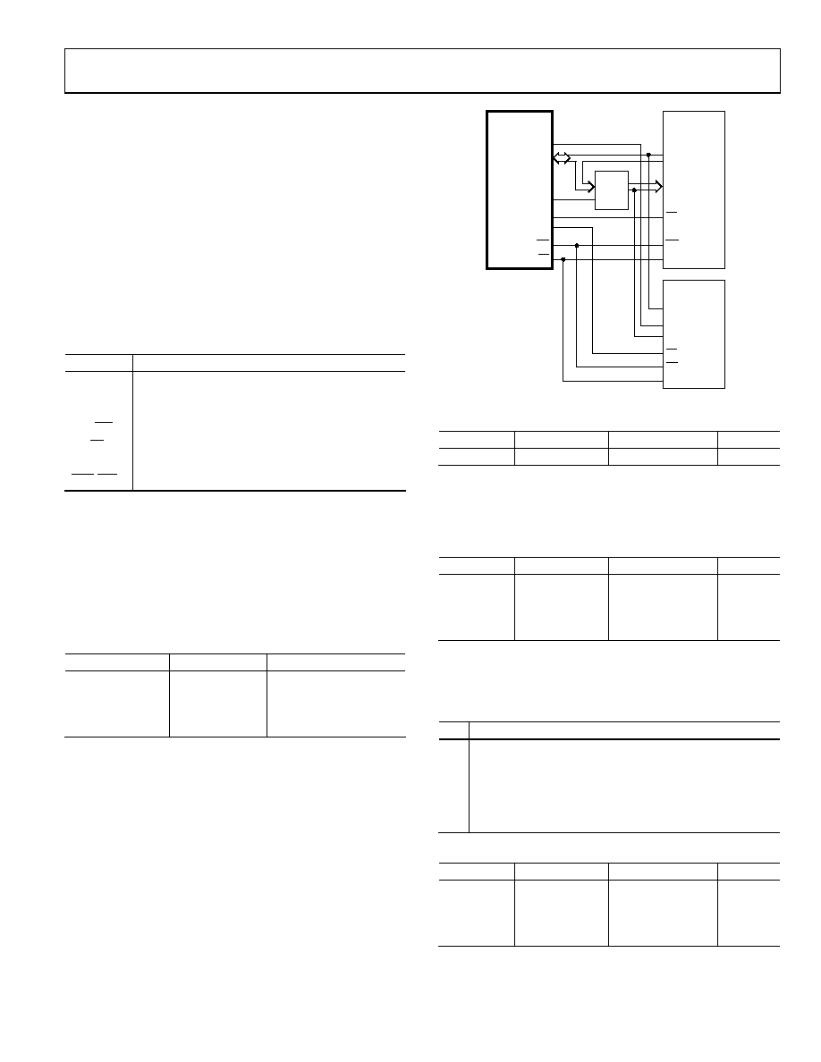
EXTERNAL MEMORY INTERFACING
The ADuC7129 is the only model in the series that features an
external memory interface. The external memory interface requires
a larger number of pins. This is why it is only available on larger
pin count packages. The XMCFG MMR must be set to 1 to use
the external port.
Although 32-bit addresses are supported internally, only the lower
16 bits of the address are on external pins.
The memory interface can address up to four 128 kB regions of
asynchronous memory (SRAM and/or EEPROM).
The pins required for interfacing to an external memory are
shown in Table 118.
Table 118. External Memory Interfacing Pins
Pin
Function
AD[15:0]
Address/Data Bus.
A16
Extended Addressing for 8-Bit Memory Only.
MS[3:0]
Memory Select.
WR (WR)
Write Strobe.
RS (RS)
Read Strobe.
AE
Address Latch Enable.
BHE, BLE
Byte Write Capability.
There are four external memory regions available, as described
in Table 119. Associated with each region are the MS[3:0] pins.
These signals allow access to the particular region of external
memory. The size of each memory region can be 128 kB
maximum, 64 k × 16, or 128 k × 8. To access 128 kB with an
8-bit memory, an extra address line (A16) is provided. (See the
example in Figure 61). The four regions are configured inde-
pendently.
Table 119. Memory Regions
Address Start
Address End
Contents
0x10000000
0x1000FFFF
External Memory 0
0x20000000
0x2000FFFF
External Memory 1
0x30000000
0x3000FFFF
External Memory 2
0x40000000
0x4000FFFF
External Memory 3
Each external memory region can be controlled through three
MMRs: XMCFG, XMxCON, and XMxPAR.
06
02
0-
0
68
LATCH
ADuC7128/
ADuC7129
AD15:0
A16
EPROM
64k × 16-BIT
A0:15
D0 TO D15
CS
RAM
128k × 8-BIT
A0:15
A16
D0 TO D7
CS
WE
OE
WE
OE
AE
MS0
MS1
WS
RS
Figure 61. Interfacing to External EPROM/RAM
XMCFG Register
Name
Address
Default Value
Access
XMCFG
0xFFFFF000
0x00
R/W
XMCFG is set to 1 to enable external memory access. This must
be set to 1 before any port pins function as external memory
access pins. The port pins must also be individually enabled via
the GPxCON MMR.
XMxCON Registers
Name
Address
Default Value
Access
XM0CON
0xFFFFF010
0x00
R/W
XM1CON
0xFFFFF014
0x00
R/W
XM2CON
0xFFFFF018
0x00
R/W
XM3CON
0xFFFFF01C
0x00
R/W
XMxCON registers are the control registers for each memory
region. They allow the enabling/disabling of a memory region
and control the data bus width of the memory region.
Table 120. XMxCON MMR Bit Designations
Bit
Description
1
Data Bus Width Select.
Set by the user to select a 16-bit data bus.
Cleared by the user to select an 8-bit data bus.
0
Memory Region Enable.
Set by the user to enable memory region.
Cleared by the user to disable the memory region.
XMxPAR Registers
Name
Address
Default Value
Access
XM0PAR
0xFFFFF020
0x70FF
R/W
XM1PAR
0xFFFFF024
0x70FF
R/W
XM2PAR
0xFFFFF028
0x70FF
R/W
XM3PAR
0xFFFFF02C
0x70FF
R/W
相关PDF资料 |
PDF描述 |
|---|---|
| VI-BTJ-IX | CONVERTER MOD DC/DC 36V 75W |
| VI-BTJ-IW | CONVERTER MOD DC/DC 36V 100W |
| VI-BTH-IX | CONVERTER MOD DC/DC 52V 75W |
| AT91SAM7X256B-CU-999 | IC MCU ARM 256KB FLASH 100TFBGA |
| VI-BT4-IW | CONVERTER MOD DC/DC 48V 100W |
相关代理商/技术参数 |
参数描述 |
|---|---|
| ADUC7128BSTZ126-RL2 | 制造商:AD 制造商全称:Analog Devices 功能描述:Precision Analog Microcontroller ARM7TDMI MCU with 12-Bit ADC and DDS DAC |
| ADUC7129 | 制造商:AD 制造商全称:Analog Devices 功能描述:Precision Analog Microcontroller ARM7TDMI MCU with 12-Bit ADC and DDS DAC |
| ADUC7129BSTZ126 | 功能描述:IC DAS MCU ARM7 ADC/DDS 80-LQFP RoHS:是 类别:集成电路 (IC) >> 嵌入式 - 微控制器, 系列:MicroConverter® ADuC7xxx 标准包装:38 系列:Encore!® XP® 核心处理器:eZ8 芯体尺寸:8-位 速度:5MHz 连通性:IrDA,UART/USART 外围设备:欠压检测/复位,LED,POR,PWM,WDT 输入/输出数:16 程序存储器容量:4KB(4K x 8) 程序存储器类型:闪存 EEPROM 大小:- RAM 容量:1K x 8 电压 - 电源 (Vcc/Vdd):2.7 V ~ 3.6 V 数据转换器:- 振荡器型:内部 工作温度:-40°C ~ 105°C 封装/外壳:20-SOIC(0.295",7.50mm 宽) 包装:管件 其它名称:269-4116Z8F0413SH005EG-ND |
| ADUC7129BSTZ1262 | 制造商:AD 制造商全称:Analog Devices 功能描述:Precision Analog Microcontroller ARM7TDMI MCU with 12-Bit ADC and DDS DAC |
| ADUC7129BSTZ126-RL | 功能描述:IC DAS MCU ARM7 ADC/DDS 80-LQFP RoHS:是 类别:集成电路 (IC) >> 嵌入式 - 微控制器, 系列:MicroConverter® ADuC7xxx 产品培训模块:Graphics LCD System and PIC24 Interface Asynchronous Stimulus 标准包装:27 系列:PIC® 24H 核心处理器:PIC 芯体尺寸:16-位 速度:40 MIP 连通性:I²C,SPI,UART/USART 外围设备:欠压检测/复位,POR,PWM,WDT 输入/输出数:21 程序存储器容量:12KB(4K x 24) 程序存储器类型:闪存 EEPROM 大小:- RAM 容量:1K x 8 电压 - 电源 (Vcc/Vdd):3 V ~ 3.6 V 数据转换器:A/D 10x10b/12b 振荡器型:内部 工作温度:-40°C ~ 85°C 封装/外壳:28-SOIC(0.295",7.50mm 宽) 包装:管件 产品目录页面:648 (CN2011-ZH PDF) 配用:AC164339-ND - MODULE SKT FOR PM3 28SOICDV164033-ND - KIT START EXPLORER 16 MPLAB ICD2 |
发布紧急采购,3分钟左右您将得到回复。