- 您现在的位置:买卖IC网 > PDF目录11203 > ADUC7128BSTZ126-RL (Analog Devices Inc)IC DAS MCU ARM7 ADC/DDS 64-LQFP PDF资料下载
参数资料
| 型号: | ADUC7128BSTZ126-RL |
| 厂商: | Analog Devices Inc |
| 文件页数: | 66/92页 |
| 文件大小: | 0K |
| 描述: | IC DAS MCU ARM7 ADC/DDS 64-LQFP |
| 产品培训模块: | ARM7 Applications & Tools Intro to ARM7 Core & Microconverters Process Control Direct Digital Synthesis Tutorial Series (1 of 7): Introduction |
| 标准包装: | 1 |
| 系列: | MicroConverter® ADuC7xxx |
| 核心处理器: | ARM7 |
| 芯体尺寸: | 16/32-位 |
| 速度: | 41.78MHz |
| 连通性: | I²C,SPI,UART/USART |
| 外围设备: | PLA,POR,PWM,PSM,温度传感器,WDT |
| 输入/输出数: | 28 |
| 程序存储器容量: | 126KB(63K x 16) |
| 程序存储器类型: | 闪存 |
| RAM 容量: | 8K x 8 |
| 电压 - 电源 (Vcc/Vdd): | 3 V ~ 3.6 V |
| 数据转换器: | A/D 10x12b; D/A 1x10b |
| 振荡器型: | 内部 |
| 工作温度: | -40°C ~ 125°C |
| 封装/外壳: | 64-LQFP |
| 包装: | 标准包装 |
| 配用: | EVAL-ADUC7128QSPZ-ND - KIT DEV FOR ADUC7128 |
| 其它名称: | ADUC7128BSTZ126-RLDKR |
第1页第2页第3页第4页第5页第6页第7页第8页第9页第10页第11页第12页第13页第14页第15页第16页第17页第18页第19页第20页第21页第22页第23页第24页第25页第26页第27页第28页第29页第30页第31页第32页第33页第34页第35页第36页第37页第38页第39页第40页第41页第42页第43页第44页第45页第46页第47页第48页第49页第50页第51页第52页第53页第54页第55页第56页第57页第58页第59页第60页第61页第62页第63页第64页第65页当前第66页第67页第68页第69页第70页第71页第72页第73页第74页第75页第76页第77页第78页第79页第80页第81页第82页第83页第84页第85页第86页第87页第88页第89页第90页第91页第92页
ADuC7128/ADuC7129
Rev. 0 | Page 69 of 92
I2CxFIF Register
Name
Address
Default Value
Access
I2C0FIF
0xFFFF084C
0x0000
R
I2C1FIF
0xFFFF094C
0x0000
R
I2CxFIF is a FIFO status register.
Table 95. I2C0FIF MMR Bit Designations
Bit
Value
Description
15:10
Reserved.
9
Master Transmit FIFO Flush.
Set by user to flush the master Tx FIFO.
Cleared automatically once the master Tx FIFO is flushed. This bit also flushes the slave receive FIFO.
8
Slave Transmit FIFO Flush.
Set by user to flush the slave Tx FIFO.
Cleared automatically once the slave Tx FIFO is flushed.
7:6
Master Rx FIFO Status Bits.
00
FIFO Empty.
01
Byte Written to FIFO.
10
1 Byte in FIFO.
11
FIFO Full.
5:4
Master Tx FIFO Status Bits.
00
FIFO Empty.
01
Byte Written to FIFO.
10
1 Byte in FIFO.
11
FIFO Full.
3:2
Slave Rx FIFO Status Bits.
00
FIFO Empty.
01
Byte Written to FIFO.
10
1 Byte in FIFO.
11
FIFO Full.
1:0
Slave Tx FIFO Status Bits.
00
FIFO Empty.
01
Byte Written to FIFO.
10
1 Byte in FIFO.
11
FIFO full.
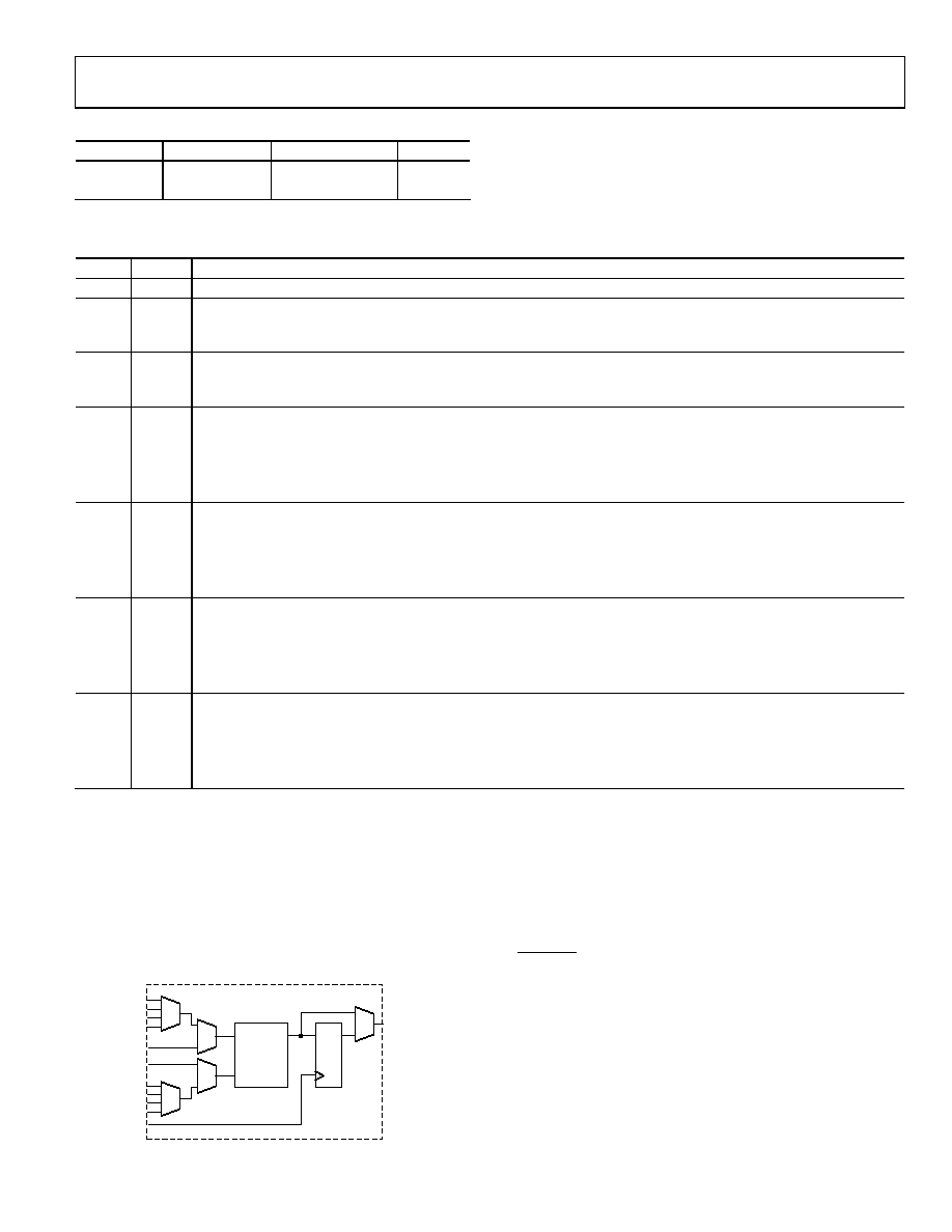
PROGRAMMABLE LOGIC ARRAY (PLA)
The ADuC7128/ADuC7129 integrate a fully programmable
logic array (PLA) that consists of two independent but
interconnected PLA blocks. Each block consists of eight PLA
elements, giving a total of 16 PLA elements.
A PLA element contains a two input look-up table that can be
configured to generate any logic output function based on two
inputs and a flip-flop as represented in Figure 54.
4
2
0
1
3
A
B
LOOK-UP
TABLE
06
02
0-
0
49
Figure 54. PLA Element
In total, 30 GPIO pins are available on the ADuC7128/ADuC7129
for the PLA. These include 16 input pins and 14 output pins.
They need to be configured in the GPxCON register as PLA
pins before using the PLA. Note that the comparator output is
also included as one of the 16 input pins.
The PLA is configured via a set of user MMRs and the output(s)
of the PLA can be routed to the internal interrupt system, to the
CONVST signal of the ADC, to an MMR, or to any of the
16 PLA output pins.
The interconnection between the two blocks is supported by
connecting the output of Element 7 of Block 1 fed back to the
Input 0 of Mux 0 of Element 0 of Block 0, and the output of
Element 7 of Block 0 is fed back to the Input 0 of Mux 0 of
Element 0 of Block 1.
相关PDF资料 |
PDF描述 |
|---|---|
| VI-BTJ-IX | CONVERTER MOD DC/DC 36V 75W |
| VI-BTJ-IW | CONVERTER MOD DC/DC 36V 100W |
| VI-BTH-IX | CONVERTER MOD DC/DC 52V 75W |
| AT91SAM7X256B-CU-999 | IC MCU ARM 256KB FLASH 100TFBGA |
| VI-BT4-IW | CONVERTER MOD DC/DC 48V 100W |
相关代理商/技术参数 |
参数描述 |
|---|---|
| ADUC7128BSTZ126-RL2 | 制造商:AD 制造商全称:Analog Devices 功能描述:Precision Analog Microcontroller ARM7TDMI MCU with 12-Bit ADC and DDS DAC |
| ADUC7129 | 制造商:AD 制造商全称:Analog Devices 功能描述:Precision Analog Microcontroller ARM7TDMI MCU with 12-Bit ADC and DDS DAC |
| ADUC7129BSTZ126 | 功能描述:IC DAS MCU ARM7 ADC/DDS 80-LQFP RoHS:是 类别:集成电路 (IC) >> 嵌入式 - 微控制器, 系列:MicroConverter® ADuC7xxx 标准包装:38 系列:Encore!® XP® 核心处理器:eZ8 芯体尺寸:8-位 速度:5MHz 连通性:IrDA,UART/USART 外围设备:欠压检测/复位,LED,POR,PWM,WDT 输入/输出数:16 程序存储器容量:4KB(4K x 8) 程序存储器类型:闪存 EEPROM 大小:- RAM 容量:1K x 8 电压 - 电源 (Vcc/Vdd):2.7 V ~ 3.6 V 数据转换器:- 振荡器型:内部 工作温度:-40°C ~ 105°C 封装/外壳:20-SOIC(0.295",7.50mm 宽) 包装:管件 其它名称:269-4116Z8F0413SH005EG-ND |
| ADUC7129BSTZ1262 | 制造商:AD 制造商全称:Analog Devices 功能描述:Precision Analog Microcontroller ARM7TDMI MCU with 12-Bit ADC and DDS DAC |
| ADUC7129BSTZ126-RL | 功能描述:IC DAS MCU ARM7 ADC/DDS 80-LQFP RoHS:是 类别:集成电路 (IC) >> 嵌入式 - 微控制器, 系列:MicroConverter® ADuC7xxx 产品培训模块:Graphics LCD System and PIC24 Interface Asynchronous Stimulus 标准包装:27 系列:PIC® 24H 核心处理器:PIC 芯体尺寸:16-位 速度:40 MIP 连通性:I²C,SPI,UART/USART 外围设备:欠压检测/复位,POR,PWM,WDT 输入/输出数:21 程序存储器容量:12KB(4K x 24) 程序存储器类型:闪存 EEPROM 大小:- RAM 容量:1K x 8 电压 - 电源 (Vcc/Vdd):3 V ~ 3.6 V 数据转换器:A/D 10x10b/12b 振荡器型:内部 工作温度:-40°C ~ 85°C 封装/外壳:28-SOIC(0.295",7.50mm 宽) 包装:管件 产品目录页面:648 (CN2011-ZH PDF) 配用:AC164339-ND - MODULE SKT FOR PM3 28SOICDV164033-ND - KIT START EXPLORER 16 MPLAB ICD2 |
发布紧急采购,3分钟左右您将得到回复。