- 您现在的位置:买卖IC网 > PDF目录11203 > ADUC7128BSTZ126-RL (Analog Devices Inc)IC DAS MCU ARM7 ADC/DDS 64-LQFP PDF资料下载
参数资料
| 型号: | ADUC7128BSTZ126-RL |
| 厂商: | Analog Devices Inc |
| 文件页数: | 26/92页 |
| 文件大小: | 0K |
| 描述: | IC DAS MCU ARM7 ADC/DDS 64-LQFP |
| 产品培训模块: | ARM7 Applications & Tools Intro to ARM7 Core & Microconverters Process Control Direct Digital Synthesis Tutorial Series (1 of 7): Introduction |
| 标准包装: | 1 |
| 系列: | MicroConverter® ADuC7xxx |
| 核心处理器: | ARM7 |
| 芯体尺寸: | 16/32-位 |
| 速度: | 41.78MHz |
| 连通性: | I²C,SPI,UART/USART |
| 外围设备: | PLA,POR,PWM,PSM,温度传感器,WDT |
| 输入/输出数: | 28 |
| 程序存储器容量: | 126KB(63K x 16) |
| 程序存储器类型: | 闪存 |
| RAM 容量: | 8K x 8 |
| 电压 - 电源 (Vcc/Vdd): | 3 V ~ 3.6 V |
| 数据转换器: | A/D 10x12b; D/A 1x10b |
| 振荡器型: | 内部 |
| 工作温度: | -40°C ~ 125°C |
| 封装/外壳: | 64-LQFP |
| 包装: | 标准包装 |
| 配用: | EVAL-ADUC7128QSPZ-ND - KIT DEV FOR ADUC7128 |
| 其它名称: | ADUC7128BSTZ126-RLDKR |
第1页第2页第3页第4页第5页第6页第7页第8页第9页第10页第11页第12页第13页第14页第15页第16页第17页第18页第19页第20页第21页第22页第23页第24页第25页当前第26页第27页第28页第29页第30页第31页第32页第33页第34页第35页第36页第37页第38页第39页第40页第41页第42页第43页第44页第45页第46页第47页第48页第49页第50页第51页第52页第53页第54页第55页第56页第57页第58页第59页第60页第61页第62页第63页第64页第65页第66页第67页第68页第69页第70页第71页第72页第73页第74页第75页第76页第77页第78页第79页第80页第81页第82页第83页第84页第85页第86页第87页第88页第89页第90页第91页第92页
ADuC7128/ADuC7129
Rev. 0 | Page 32 of 92
ADC CIRCUIT OVERVIEW
The analog-to-digital converter (ADC) incorporates a fast,
multichannel, 12-bit ADC. It can operate from 3.0 V to 3.6 V
supplies and is capable of providing a throughput of up to 1 MSPS
when the clock source is 41.78 MHz. This block provides the
user with a multichannel multiplexer, differential track-and-
hold, on-chip reference, and ADC.
The ADC consists of a 12-bit successive approximation converter
based around two capacitor DACs. Depending on the input
signal configuration, the ADC can operate in one of the
following three modes:
Fully differential mode, for small and balanced signals
Single-ended mode, for any single-ended signals
Pseudo differential mode, for any single-ended signals,
taking advantage of the common mode rejection offered by
the pseudo differential input
The converter accepts an analog input range of 0 to VREF when
operating in single-ended mode or pseudo differential mode. In
fully differential mode, the input signal must be balanced around
a common-mode voltage VCM, in the range 0 V to AVDD and
AVDD
VCM
0
2VREF
0
60
20
-02
8
Figure 32. Examples of Balanced Signals for Fully Differential Mode
A high precision, low drift, and factory-calibrated 2.5 V reference
is provided on-chip. An external reference can also be connected
as described in the Band Gap Reference section.
Single or continuous conversion modes can be initiated in software.
An external CONVST pin, an output generated from the on-chip
PLA, a Timer0, or a Timer1 overflow can also be used to
generate a repetitive trigger for ADC conversions.
If the signal has not been deasserted by the time the ADC
conversion is complete, a second conversion begins auto-
matically.
A voltage output from an on-chip band gap reference propor-
tional to absolute temperature can also be routed through the
front-end ADC multiplexer, effectively an additional ADC
channel input. This facilitates an internal temperature sensor
channel, measuring die temperature to an accuracy of ±3°C.
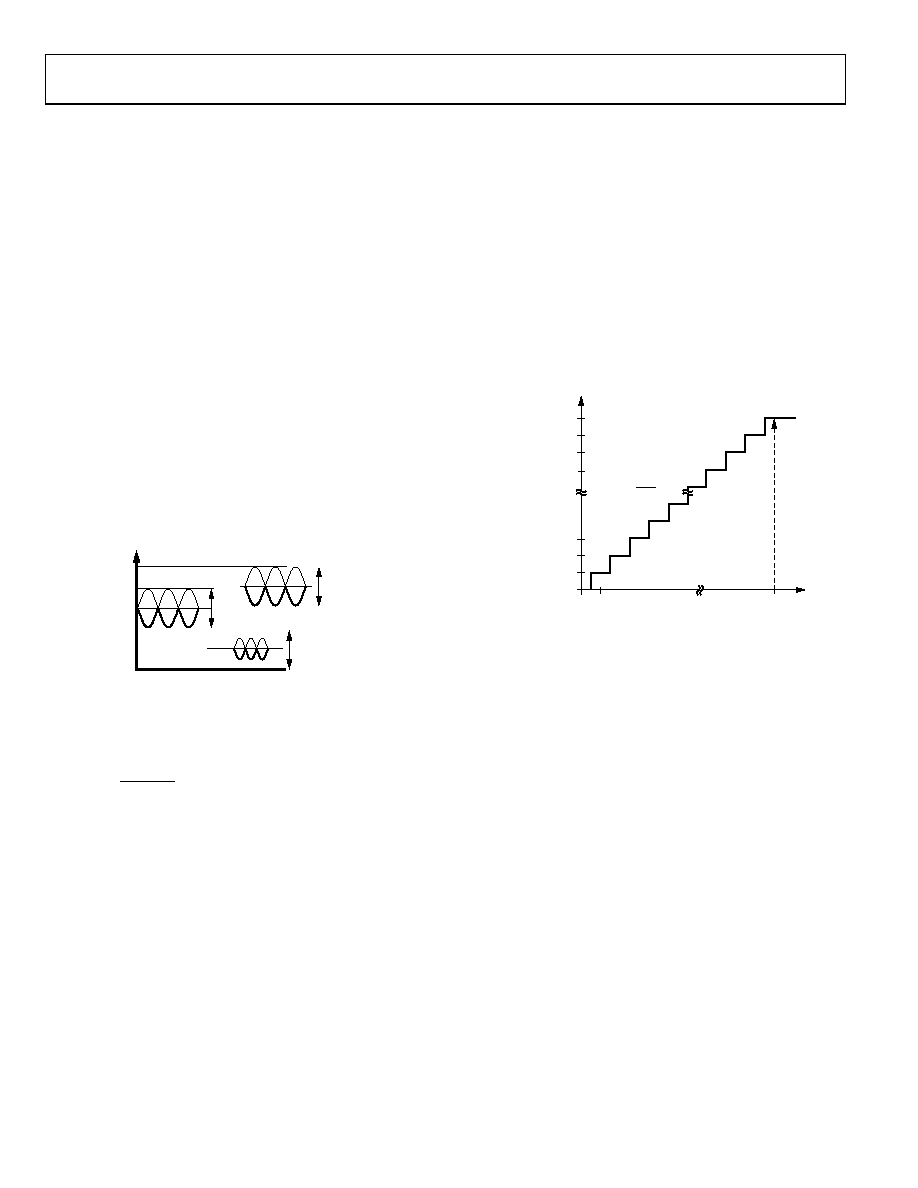
ADC TRANSFER FUNCTION
Pseudo Differential Mode and Single-Ended Mode
In pseudo differential or single-ended mode, the input range is
0 to VREF. The output coding is straight binary in pseudo
differential and single-ended modes with
1 LSB = FS/4096 or
2.5 V/4096 = 0.61 mV or
610 μV when VREF = 2.5 V
The ideal code transitions occur midway between successive
integer LSB values (that is, 1/2 LSB, 3/2 LSBs, 5/2 LSBs, …,
FS – 3/2 LSBs). The ideal input/output transfer characteristic is
shown in Figure 33.
O
U
T
P
UT
CO
DE
VOLTAGE INPUT
1111 1111 1111
1111 1111 1110
1111 1111 1101
1111 1111 1100
0000 0000 0011
1LSB
0V
+FS – 1LSB
0000 0000 0010
0000 0000 0001
0000 0000 0000
1LSB =
FS
4096
06
02
0-
0
29
Figure 33. ADC Transfer Function in Pseudo Differential Mode or
Single-Ended Mode
Fully Differential Mode
The amplitude of the differential signal is the difference
between the signals applied to the VIN+ and VIN pins (that is,
VIN+ VIN). The maximum amplitude of the differential signal
is, therefore, VREF to +VREF p-p (2 × VREF). This is regardless of
the common mode (CM). The common mode is the average of
the two signals (VIN+ + VIN)/2, and is, therefore, the voltage upon
which the two inputs are centered. This results in the span of
each input being CM ± VREF/2. This voltage has to be set up exter-
Inputs section).
The output coding is twos complement in fully differential
mode with 1 LSB = 2 VREF/4096 or 2 × 2.5 V/4096 = 1.22 mV
when VREF = 2.5 V. The output result is ±11 bits, but this is
shifted by one to the right. This allows the result in ADCDAT to
be declared as a signed integer when writing C code. The
designed code transitions occur midway between successive
integer LSB values (that is, 1/2 LSB, 3/2 LSBs, 5/2 LSBs, …,
FS 3/2 LSBs). The ideal input/output transfer characteristic is
shown in Figure 34.
相关PDF资料 |
PDF描述 |
|---|---|
| VI-BTJ-IX | CONVERTER MOD DC/DC 36V 75W |
| VI-BTJ-IW | CONVERTER MOD DC/DC 36V 100W |
| VI-BTH-IX | CONVERTER MOD DC/DC 52V 75W |
| AT91SAM7X256B-CU-999 | IC MCU ARM 256KB FLASH 100TFBGA |
| VI-BT4-IW | CONVERTER MOD DC/DC 48V 100W |
相关代理商/技术参数 |
参数描述 |
|---|---|
| ADUC7128BSTZ126-RL2 | 制造商:AD 制造商全称:Analog Devices 功能描述:Precision Analog Microcontroller ARM7TDMI MCU with 12-Bit ADC and DDS DAC |
| ADUC7129 | 制造商:AD 制造商全称:Analog Devices 功能描述:Precision Analog Microcontroller ARM7TDMI MCU with 12-Bit ADC and DDS DAC |
| ADUC7129BSTZ126 | 功能描述:IC DAS MCU ARM7 ADC/DDS 80-LQFP RoHS:是 类别:集成电路 (IC) >> 嵌入式 - 微控制器, 系列:MicroConverter® ADuC7xxx 标准包装:38 系列:Encore!® XP® 核心处理器:eZ8 芯体尺寸:8-位 速度:5MHz 连通性:IrDA,UART/USART 外围设备:欠压检测/复位,LED,POR,PWM,WDT 输入/输出数:16 程序存储器容量:4KB(4K x 8) 程序存储器类型:闪存 EEPROM 大小:- RAM 容量:1K x 8 电压 - 电源 (Vcc/Vdd):2.7 V ~ 3.6 V 数据转换器:- 振荡器型:内部 工作温度:-40°C ~ 105°C 封装/外壳:20-SOIC(0.295",7.50mm 宽) 包装:管件 其它名称:269-4116Z8F0413SH005EG-ND |
| ADUC7129BSTZ1262 | 制造商:AD 制造商全称:Analog Devices 功能描述:Precision Analog Microcontroller ARM7TDMI MCU with 12-Bit ADC and DDS DAC |
| ADUC7129BSTZ126-RL | 功能描述:IC DAS MCU ARM7 ADC/DDS 80-LQFP RoHS:是 类别:集成电路 (IC) >> 嵌入式 - 微控制器, 系列:MicroConverter® ADuC7xxx 产品培训模块:Graphics LCD System and PIC24 Interface Asynchronous Stimulus 标准包装:27 系列:PIC® 24H 核心处理器:PIC 芯体尺寸:16-位 速度:40 MIP 连通性:I²C,SPI,UART/USART 外围设备:欠压检测/复位,POR,PWM,WDT 输入/输出数:21 程序存储器容量:12KB(4K x 24) 程序存储器类型:闪存 EEPROM 大小:- RAM 容量:1K x 8 电压 - 电源 (Vcc/Vdd):3 V ~ 3.6 V 数据转换器:A/D 10x10b/12b 振荡器型:内部 工作温度:-40°C ~ 85°C 封装/外壳:28-SOIC(0.295",7.50mm 宽) 包装:管件 产品目录页面:648 (CN2011-ZH PDF) 配用:AC164339-ND - MODULE SKT FOR PM3 28SOICDV164033-ND - KIT START EXPLORER 16 MPLAB ICD2 |
发布紧急采购,3分钟左右您将得到回复。