- 您现在的位置:买卖IC网 > PDF目录11203 > ADUC7128BSTZ126-RL (Analog Devices Inc)IC DAS MCU ARM7 ADC/DDS 64-LQFP PDF资料下载
参数资料
| 型号: | ADUC7128BSTZ126-RL |
| 厂商: | Analog Devices Inc |
| 文件页数: | 35/92页 |
| 文件大小: | 0K |
| 描述: | IC DAS MCU ARM7 ADC/DDS 64-LQFP |
| 产品培训模块: | ARM7 Applications & Tools Intro to ARM7 Core & Microconverters Process Control Direct Digital Synthesis Tutorial Series (1 of 7): Introduction |
| 标准包装: | 1 |
| 系列: | MicroConverter® ADuC7xxx |
| 核心处理器: | ARM7 |
| 芯体尺寸: | 16/32-位 |
| 速度: | 41.78MHz |
| 连通性: | I²C,SPI,UART/USART |
| 外围设备: | PLA,POR,PWM,PSM,温度传感器,WDT |
| 输入/输出数: | 28 |
| 程序存储器容量: | 126KB(63K x 16) |
| 程序存储器类型: | 闪存 |
| RAM 容量: | 8K x 8 |
| 电压 - 电源 (Vcc/Vdd): | 3 V ~ 3.6 V |
| 数据转换器: | A/D 10x12b; D/A 1x10b |
| 振荡器型: | 内部 |
| 工作温度: | -40°C ~ 125°C |
| 封装/外壳: | 64-LQFP |
| 包装: | 标准包装 |
| 配用: | EVAL-ADUC7128QSPZ-ND - KIT DEV FOR ADUC7128 |
| 其它名称: | ADUC7128BSTZ126-RLDKR |
第1页第2页第3页第4页第5页第6页第7页第8页第9页第10页第11页第12页第13页第14页第15页第16页第17页第18页第19页第20页第21页第22页第23页第24页第25页第26页第27页第28页第29页第30页第31页第32页第33页第34页当前第35页第36页第37页第38页第39页第40页第41页第42页第43页第44页第45页第46页第47页第48页第49页第50页第51页第52页第53页第54页第55页第56页第57页第58页第59页第60页第61页第62页第63页第64页第65页第66页第67页第68页第69页第70页第71页第72页第73页第74页第75页第76页第77页第78页第79页第80页第81页第82页第83页第84页第85页第86页第87页第88页第89页第90页第91页第92页
ADuC7128/ADuC7129
Rev. 0 | Page 40 of 92
FLASH/EE MEMORY SECURITY
The 126 kB of Flash/EE memory available to the user can be
read and write protected. Bit 31 of the FEE0PRO/FEE0HID MMR
protects the 126 kB from being read through JTAG and also in
parallel programming mode. The other 31 bits of this register
protect writing to the Flash/EE memory; each bit protects four
pages, that is, 2 kB. Write protection is activated for all access types.
FEE1PRO and FEE1HID similarly protect the second 64 kB block.
All 32 bits of this are used to protect four pages at a time.
Three Levels of Protection
Protection can be set and removed by writing directly into
FEExHID MMR. This protection does not remain after reset.
Protection can be set by writing into FEExPRO MMR. It takes
effect only after a save protection command (0x0C) and a reset.
The FEExPRO MMR is protected by a key to avoid direct access.
The key is saved once and must be entered again to modify
FEExPRO. A mass erase sets the key back to 0xFFFF but also
erases all the user code.
The Flash/EE memory can be permanently protected by using
the FEEPRO MMR and a particular value of the 0xDEADDEAD
key. Entering the key again to modify the FEExPRO register is
not allowed.
Sequence to Write the Key
1.
Write the bit in FEExPRO corresponding to the page to be
protected.
2.
Enable key protection by setting Bit 6 of FEExMOD (Bit 5
must equal 0).
3.
Write a 32-bit key in FEExADR, FEExDAT.
4.
Run the write key command 0×0C in FEExCON; wait for
the read to be successful by monitoring FEExSTA.
5.
Reset the part.
To remove or modify the protection, the same sequence is used
with a modified value of FEExPRO. If the key chosen is the value
0xDEAD, then the memory protection cannot be removed. Only
a mass erase unprotects the part, but it also erases all user code.
The sequence to write the key is shown in the following example;
this protects writing Page 4 to Page 7 of the Flash/EE memory:
FEE0PRO=0xFFFFFFFD;
//Protect pages 4 to 7
FEE0MOD=0x48;
//Write key enable
FEE0ADR=0x1234;
//16 bit key value
FEE0DAT=0x5678;
//16 bit key value
FEE0CON= 0x0C;
// Write key command
The same sequence should be followed to protect the part
permanently with FEExADR = 0xDEAD and FEExDAT =
0xDEAD.
FLASH/EE CONTROL INTERFACE
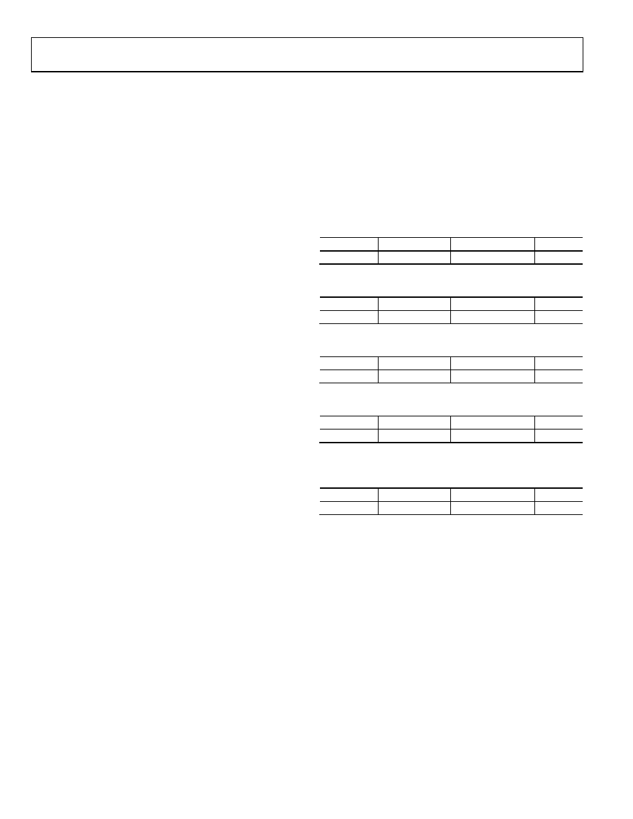
FEE0DAT Register
Name
Address
Default Value
Access
FEE0DAT
0xFFFF0E0C
0xXXXX
R/W
FEE0DAT is a 16-bit data register.
FEE0ADR Register
Name
Address
Default Value
Access
FEE0ADR
0xFFFF0E10
0x0000
R/W
FEE0ADR is a 16-bit address register.
FEE0SGN Register
Name
Address
Default Value
Access
FEE0SGN
0xFFFF0E18
0xFFFFFF
R
FEE0SGN is a 24-bit code signature.
FEE0PRO Register
Name
Address
Default Value
Access
FEE0PRO
0xFFFF0E1C
0x00000000
R/W
FEE0PRO provides protection following subsequent reset MMR.
It requires a software key (see Table 44).
FEE0HID Register
Name
Address
Default Value
Access
FEE0HID
0xFFFF0E20
0xFFFFFFFF
R/W
FEE0HID provides immediate protection MMR. It does not
require any software keys (see Table 44).
Command Sequence for Executing a Mass Erase
FEE0DAT = 0x3CFF;
FEE0ADR = 0xFFC3;
FEE0MOD = FEE0MOD|0x8;
//Erase key enable
FEE0CON = 0x06;
//Mass erase command
相关PDF资料 |
PDF描述 |
|---|---|
| VI-BTJ-IX | CONVERTER MOD DC/DC 36V 75W |
| VI-BTJ-IW | CONVERTER MOD DC/DC 36V 100W |
| VI-BTH-IX | CONVERTER MOD DC/DC 52V 75W |
| AT91SAM7X256B-CU-999 | IC MCU ARM 256KB FLASH 100TFBGA |
| VI-BT4-IW | CONVERTER MOD DC/DC 48V 100W |
相关代理商/技术参数 |
参数描述 |
|---|---|
| ADUC7128BSTZ126-RL2 | 制造商:AD 制造商全称:Analog Devices 功能描述:Precision Analog Microcontroller ARM7TDMI MCU with 12-Bit ADC and DDS DAC |
| ADUC7129 | 制造商:AD 制造商全称:Analog Devices 功能描述:Precision Analog Microcontroller ARM7TDMI MCU with 12-Bit ADC and DDS DAC |
| ADUC7129BSTZ126 | 功能描述:IC DAS MCU ARM7 ADC/DDS 80-LQFP RoHS:是 类别:集成电路 (IC) >> 嵌入式 - 微控制器, 系列:MicroConverter® ADuC7xxx 标准包装:38 系列:Encore!® XP® 核心处理器:eZ8 芯体尺寸:8-位 速度:5MHz 连通性:IrDA,UART/USART 外围设备:欠压检测/复位,LED,POR,PWM,WDT 输入/输出数:16 程序存储器容量:4KB(4K x 8) 程序存储器类型:闪存 EEPROM 大小:- RAM 容量:1K x 8 电压 - 电源 (Vcc/Vdd):2.7 V ~ 3.6 V 数据转换器:- 振荡器型:内部 工作温度:-40°C ~ 105°C 封装/外壳:20-SOIC(0.295",7.50mm 宽) 包装:管件 其它名称:269-4116Z8F0413SH005EG-ND |
| ADUC7129BSTZ1262 | 制造商:AD 制造商全称:Analog Devices 功能描述:Precision Analog Microcontroller ARM7TDMI MCU with 12-Bit ADC and DDS DAC |
| ADUC7129BSTZ126-RL | 功能描述:IC DAS MCU ARM7 ADC/DDS 80-LQFP RoHS:是 类别:集成电路 (IC) >> 嵌入式 - 微控制器, 系列:MicroConverter® ADuC7xxx 产品培训模块:Graphics LCD System and PIC24 Interface Asynchronous Stimulus 标准包装:27 系列:PIC® 24H 核心处理器:PIC 芯体尺寸:16-位 速度:40 MIP 连通性:I²C,SPI,UART/USART 外围设备:欠压检测/复位,POR,PWM,WDT 输入/输出数:21 程序存储器容量:12KB(4K x 24) 程序存储器类型:闪存 EEPROM 大小:- RAM 容量:1K x 8 电压 - 电源 (Vcc/Vdd):3 V ~ 3.6 V 数据转换器:A/D 10x10b/12b 振荡器型:内部 工作温度:-40°C ~ 85°C 封装/外壳:28-SOIC(0.295",7.50mm 宽) 包装:管件 产品目录页面:648 (CN2011-ZH PDF) 配用:AC164339-ND - MODULE SKT FOR PM3 28SOICDV164033-ND - KIT START EXPLORER 16 MPLAB ICD2 |
发布紧急采购,3分钟左右您将得到回复。