- 您现在的位置:买卖IC网 > PDF目录11203 > ADUC7128BSTZ126-RL (Analog Devices Inc)IC DAS MCU ARM7 ADC/DDS 64-LQFP PDF资料下载
参数资料
| 型号: | ADUC7128BSTZ126-RL |
| 厂商: | Analog Devices Inc |
| 文件页数: | 42/92页 |
| 文件大小: | 0K |
| 描述: | IC DAS MCU ARM7 ADC/DDS 64-LQFP |
| 产品培训模块: | ARM7 Applications & Tools Intro to ARM7 Core & Microconverters Process Control Direct Digital Synthesis Tutorial Series (1 of 7): Introduction |
| 标准包装: | 1 |
| 系列: | MicroConverter® ADuC7xxx |
| 核心处理器: | ARM7 |
| 芯体尺寸: | 16/32-位 |
| 速度: | 41.78MHz |
| 连通性: | I²C,SPI,UART/USART |
| 外围设备: | PLA,POR,PWM,PSM,温度传感器,WDT |
| 输入/输出数: | 28 |
| 程序存储器容量: | 126KB(63K x 16) |
| 程序存储器类型: | 闪存 |
| RAM 容量: | 8K x 8 |
| 电压 - 电源 (Vcc/Vdd): | 3 V ~ 3.6 V |
| 数据转换器: | A/D 10x12b; D/A 1x10b |
| 振荡器型: | 内部 |
| 工作温度: | -40°C ~ 125°C |
| 封装/外壳: | 64-LQFP |
| 包装: | 标准包装 |
| 配用: | EVAL-ADUC7128QSPZ-ND - KIT DEV FOR ADUC7128 |
| 其它名称: | ADUC7128BSTZ126-RLDKR |
第1页第2页第3页第4页第5页第6页第7页第8页第9页第10页第11页第12页第13页第14页第15页第16页第17页第18页第19页第20页第21页第22页第23页第24页第25页第26页第27页第28页第29页第30页第31页第32页第33页第34页第35页第36页第37页第38页第39页第40页第41页当前第42页第43页第44页第45页第46页第47页第48页第49页第50页第51页第52页第53页第54页第55页第56页第57页第58页第59页第60页第61页第62页第63页第64页第65页第66页第67页第68页第69页第70页第71页第72页第73页第74页第75页第76页第77页第78页第79页第80页第81页第82页第83页第84页第85页第86页第87页第88页第89页第90页第91页第92页
ADuC7128/ADuC7129
Rev. 0 | Page 47 of 92
DDSFRQ Register
Name
Address
Default Value
Access
DDSFRQ
0xFFFF0694
0x00000000
R/W
Table 54. DDSFRQ MMR Bit Designations
Bit
Description
31:0
Frequency select word (FSW)
The DDS frequency is controlled via the DDSFRQ MMR. This
MMR contains a 32-bit word (FSW) that controls the frequency
according to the following formula:
32
2
MHz
8896
.
20
×
=
FSW
Frequency
DDSPHS Register
Name
Address
Default Value
Access
DDSPHS
0xFFFF0698
0x00000000
R/W
Table 55. DDSPHS MMR Bit Designations
Bit
Description
31:12
Reserved
11:0
Phase
The DDS phase offset is controlled via the DDSPHS MMR. This
MMR contains a 12-bit value that controls the phase of the DDS
output according to the following formula:
12
2
Phase
Offset
Phase
×
π
×
=
POWER SUPPLY MONITOR
The power supply monitor on the ADuC7128/ADuC7129
indicates when the IOVDD supply pin drops below one of two
supply trip points. The monitor function is controlled via the
PSMCON register (see Table 56). If enabled in the IRQEN or
FIQEN register, the monitor interrupts the core using the PSMI
bit in the PSMCON MMR. This bit is cleared immediately once
CMP goes high. Note that if the interrupt generated is exited
before CMP goes high (IOVDD is above the trip point), no further
interrupts are generated until CMP returns high. The user should
ensure that code execution remains within the ISR until CMP
returns high.
This monitor function allows the user to save working registers
to avoid possible data loss due to the low supply or brown-out
conditions. It also ensures that normal code execution does not
resume until a safe supply level has been established.
The PSM does not operate correctly when using JTAG debug.
It should be disabled in JTAG debug mode.
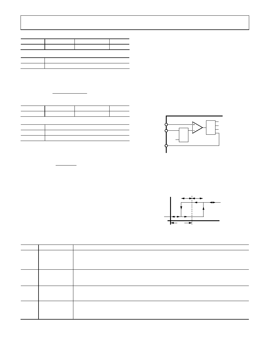
COMPARATOR
The ADuC7128/ADuC7129 integrate an uncommitted voltage
comparator. The positive input is multiplexed with ADC2, and
the negative input has two options: ADC3 or the internal refer-
ence. The output of the comparator can be configured to generate
a system interrupt, can be routed directly to the programmable
logic array, can start an ADC conversion, or can be on an
external pin, CMPOUT.
MUX
CONVERSION
MUX
REF
PLA
IRQ
ADC START
ADC2/CMP0
ADC3/CMP1
P0.0/CMPOUT
06
02
0-
04
2
Figure 46. Comparator
Hysteresis
Figure 47 shows how the input offset voltage and hysteresis
terms are defined. Input offset voltage (VOS) is the difference
between the center of the hysteresis range and the ground level.
This can either be positive or negative. The hysteresis voltage
(VH) is the width of the hysteresis range.
COMPOUT
COMP0
VH
VOS
0
60
20
-0
41
Figure 47. Comparator Hysteresis Transfer Function
Table 56. PSMCON MMR Bit Designations
Bit
Name
Description
3
CMP
Comparator Bit. This is a read-only bit that directly reflects the state of the comparator.
Read 1 indicates the IOVDD supply is above its selected trip point or the PSM is in power-down mode.
Read 0 indicates the IOVDD supply is below its selected trip point. This bit should be set before leaving
the interrupt service routine.
Trip Point Selection Bit.
0 = 2.79 V
2
TP
1 = 3.07 V
1
PSMEN
Power Supply Monitor Enable Bit.
Set to 1 by the user to enable the power supply monitor circuit.
Cleared to 0 by the user to disable the power supply monitor circuit.
0
PSMI
Power Supply Monitor Interrupt Bit. This bit is set high by the MicroConverter if CMP is low, indicating low
I/O supply. The PSMI bit can be used to interrupt the processor. Once CMP returns high, the PSMI bit can
be cleared by writing a 1 to this location. A write of 0 has no effect. There is no timeout delay. PSMI can be
cleared immediately once CMP goes high.
相关PDF资料 |
PDF描述 |
|---|---|
| VI-BTJ-IX | CONVERTER MOD DC/DC 36V 75W |
| VI-BTJ-IW | CONVERTER MOD DC/DC 36V 100W |
| VI-BTH-IX | CONVERTER MOD DC/DC 52V 75W |
| AT91SAM7X256B-CU-999 | IC MCU ARM 256KB FLASH 100TFBGA |
| VI-BT4-IW | CONVERTER MOD DC/DC 48V 100W |
相关代理商/技术参数 |
参数描述 |
|---|---|
| ADUC7128BSTZ126-RL2 | 制造商:AD 制造商全称:Analog Devices 功能描述:Precision Analog Microcontroller ARM7TDMI MCU with 12-Bit ADC and DDS DAC |
| ADUC7129 | 制造商:AD 制造商全称:Analog Devices 功能描述:Precision Analog Microcontroller ARM7TDMI MCU with 12-Bit ADC and DDS DAC |
| ADUC7129BSTZ126 | 功能描述:IC DAS MCU ARM7 ADC/DDS 80-LQFP RoHS:是 类别:集成电路 (IC) >> 嵌入式 - 微控制器, 系列:MicroConverter® ADuC7xxx 标准包装:38 系列:Encore!® XP® 核心处理器:eZ8 芯体尺寸:8-位 速度:5MHz 连通性:IrDA,UART/USART 外围设备:欠压检测/复位,LED,POR,PWM,WDT 输入/输出数:16 程序存储器容量:4KB(4K x 8) 程序存储器类型:闪存 EEPROM 大小:- RAM 容量:1K x 8 电压 - 电源 (Vcc/Vdd):2.7 V ~ 3.6 V 数据转换器:- 振荡器型:内部 工作温度:-40°C ~ 105°C 封装/外壳:20-SOIC(0.295",7.50mm 宽) 包装:管件 其它名称:269-4116Z8F0413SH005EG-ND |
| ADUC7129BSTZ1262 | 制造商:AD 制造商全称:Analog Devices 功能描述:Precision Analog Microcontroller ARM7TDMI MCU with 12-Bit ADC and DDS DAC |
| ADUC7129BSTZ126-RL | 功能描述:IC DAS MCU ARM7 ADC/DDS 80-LQFP RoHS:是 类别:集成电路 (IC) >> 嵌入式 - 微控制器, 系列:MicroConverter® ADuC7xxx 产品培训模块:Graphics LCD System and PIC24 Interface Asynchronous Stimulus 标准包装:27 系列:PIC® 24H 核心处理器:PIC 芯体尺寸:16-位 速度:40 MIP 连通性:I²C,SPI,UART/USART 外围设备:欠压检测/复位,POR,PWM,WDT 输入/输出数:21 程序存储器容量:12KB(4K x 24) 程序存储器类型:闪存 EEPROM 大小:- RAM 容量:1K x 8 电压 - 电源 (Vcc/Vdd):3 V ~ 3.6 V 数据转换器:A/D 10x10b/12b 振荡器型:内部 工作温度:-40°C ~ 85°C 封装/外壳:28-SOIC(0.295",7.50mm 宽) 包装:管件 产品目录页面:648 (CN2011-ZH PDF) 配用:AC164339-ND - MODULE SKT FOR PM3 28SOICDV164033-ND - KIT START EXPLORER 16 MPLAB ICD2 |
发布紧急采购,3分钟左右您将得到回复。