- 您现在的位置:买卖IC网 > PDF目录294982 > AGLN250V2-CS81 FPGA, 6144 CLBS, 250000 GATES, 250 MHz, PBGA81 PDF资料下载
参数资料
| 型号: | AGLN250V2-CS81 |
| 元件分类: | FPGA |
| 英文描述: | FPGA, 6144 CLBS, 250000 GATES, 250 MHz, PBGA81 |
| 封装: | 5 X 5 MM, 0.8 MM HEIGHT, 0.5 MM PITCH, CSP-81 |
| 文件页数: | 125/140页 |
| 文件大小: | 4325K |
| 代理商: | AGLN250V2-CS81 |
第1页第2页第3页第4页第5页第6页第7页第8页第9页第10页第11页第12页第13页第14页第15页第16页第17页第18页第19页第20页第21页第22页第23页第24页第25页第26页第27页第28页第29页第30页第31页第32页第33页第34页第35页第36页第37页第38页第39页第40页第41页第42页第43页第44页第45页第46页第47页第48页第49页第50页第51页第52页第53页第54页第55页第56页第57页第58页第59页第60页第61页第62页第63页第64页第65页第66页第67页第68页第69页第70页第71页第72页第73页第74页第75页第76页第77页第78页第79页第80页第81页第82页第83页第84页第85页第86页第87页第88页第89页第90页第91页第92页第93页第94页第95页第96页第97页第98页第99页第100页第101页第102页第103页第104页第105页第106页第107页第108页第109页第110页第111页第112页第113页第114页第115页第116页第117页第118页第119页第120页第121页第122页第123页第124页当前第125页第126页第127页第128页第129页第130页第131页第132页第133页第134页第135页第136页第137页第138页第139页第140页
IGLOO nano Low Power Flash FPGAs
Re vi s i on 10
2 - 71
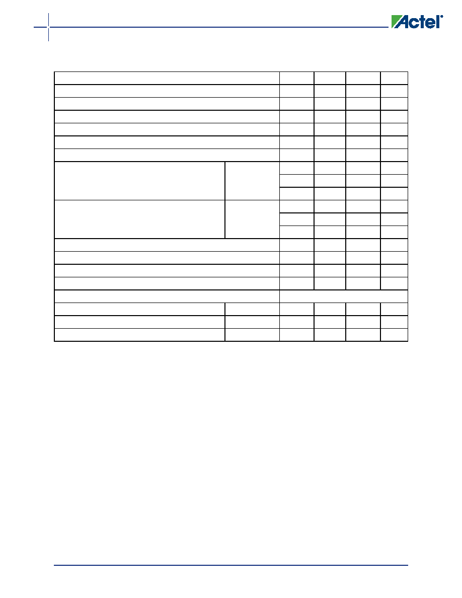
Table 2-102 IGLOO nano CCC/PLL Specification
For IGLOO nano V2 Devices, 1.2 V DC Core Supply Voltage
Parameter
Min.
Typ.
Max.
Units
Clock Conditioning Circuitry Input Frequency fIN_CCC
1.5
160
MHz
Clock Conditioning Circuitry Output Frequency fOUT_CCC
0.75
160
MHz
Delay Increments in Programmable Delay Blocks 1, 2
580
ps
Number of Programmable Values in Each Programmable Delay Block
32
Serial Clock (SCLK) for Dynamic PLL 3
60
Input Cycle-to-Cycle Jitter (peak magnitude)
0.25
ns
Acquisition Time
LockControl = 0
300
s
LockControl = 1
6.0
ms
Tracking Jitter 4
LockControl = 0
4
ns
LockControl = 1
3
ns
Output Duty Cycle
48.5
51.5
%
Delay Range in Block: Programmable Delay 1 1, 2
2.3
20.86
ns
Delay Range in Block: Programmable Delay 2 1, 2
0.025
20.86
ns
Delay Range in Block: Fixed Delay 1, 2
5.7
ns
VCO Output Peak-to-Peak Period Jitter FCCC_OUT
5
Max Peak-to-Peak Period Jitter 5,6,7
SSO
≤ 2SSO ≤ 4 SSO ≤ 8SSO ≤ 16
0.75 MHz to 50MHz
0.50
1.20
2.00
3.00
%
50 MHz to 100 MHz
2.50
5.00
7.00
15.00
%
Notes:
1. This delay is a function of voltage and temperature. See Table 2-6 on page 2-6 and Table 2-7 on page 2-7 for deratings.
2. TJ = 25°C, VCC = 1.2 V
3. Maximum value obtained for a STD speed grade device in Worst-Case Commercial conditions. For specific junction
temperature and voltage supply levels, refer to Table 2-6 on page 2-6 and Table 2-7 on page 2-7 for derating values.
4. Tracking jitter is defined as the variation in clock edge position of PLL outputs with reference to the PLL input clock
edge. Tracking jitter does not measure the variation in PLL output period, which is covered by the period jitter
parameter.
5. VCO output jitter is calculated as a percentage of the VCO frequency. The jitter (in ps) can be calculated by multiplying
the VCO period by the % jitter. The VCO jitter (in ps) applies to CCC_OUT, regardless of the output divider settings. For
example, if the jitter on VCO is 300 ps, the jitter on CCC_OUT is also 300 ps, no matter what the settings are for the
output divider.
6. Measurements done with LVTTL 3.3 V 8 mA I/O drive strength and high slew rate. VCC/VCCPLL = 1.14 V,
VCCI = 3.3 V, VQ/PQ/TQ type of packages, 20 pF load.
7. SSOs are outputs that are synchronous to a single clock domain and have their clock-to-out times within ±200 ps of
each other. Switching I/Os are placed outside of the PLL bank. Refer to ProASIC3/E SSO and Pin Placement
8. The AGLN010, AGLN015, and AGLN020 devices do not support PLLs.
相关PDF资料 |
PDF描述 |
|---|---|
| AGLN250V2-ZCS81I | FPGA, 6144 CLBS, 250000 GATES, 250 MHz, PBGA81 |
| AGLN250V2-ZCS81 | FPGA, 6144 CLBS, 250000 GATES, 250 MHz, PBGA81 |
| AGLN030V2-ZCS81I | FPGA, 768 CLBS, 30000 GATES, 250 MHz, PBGA81 |
| AGLN030V2-ZCS81 | FPGA, 768 CLBS, 30000 GATES, 250 MHz, PBGA81 |
| AGLN030V2-ZQN48I | FPGA, 768 CLBS, 30000 GATES, 250 MHz, QCC48 |
相关代理商/技术参数 |
参数描述 |
|---|---|
| AGLN250V2-CSG81 | 功能描述:IC FPGA 250K 1.2-1.5V CSP81 RoHS:是 类别:集成电路 (IC) >> 嵌入式 - FPGA(现场可编程门阵列) 系列:IGLOO nano 标准包装:24 系列:ECP2 LAB/CLB数:1500 逻辑元件/单元数:12000 RAM 位总计:226304 输入/输出数:131 门数:- 电源电压:1.14 V ~ 1.26 V 安装类型:表面贴装 工作温度:0°C ~ 85°C 封装/外壳:208-BFQFP 供应商设备封装:208-PQFP(28x28) |
| AGLN250V2-CSG81I | 功能描述:IC FPGA NANO 1KB 250K 81-CSP RoHS:是 类别:集成电路 (IC) >> 嵌入式 - FPGA(现场可编程门阵列) 系列:IGLOO nano 标准包装:152 系列:IGLOO PLUS LAB/CLB数:- 逻辑元件/单元数:792 RAM 位总计:- 输入/输出数:120 门数:30000 电源电压:1.14 V ~ 1.575 V 安装类型:表面贴装 工作温度:-40°C ~ 85°C 封装/外壳:289-TFBGA,CSBGA 供应商设备封装:289-CSP(14x14) |
| AGLN250V2-DIELOT | 制造商:Microsemi Corporation 功能描述:AGLN250V2-DIELOT - Gel-pak, waffle pack, wafer, diced wafer on film 制造商:Microsemi SOC Products Group 功能描述:AGLN250V2-DIELOT - Gel-pak, waffle pack, wafer, diced wafer on film |
| AGLN250V2-QNG100I | 制造商:Microsemi Corporation 功能描述:FPGA IGLOO NANO FAMILY 250K GATES 130NM (CMOS) TECHNOLOGY 1. - Trays |
| AGLN250V2-VQ100 | 功能描述:IC FPGA NANO 1KB 250K 100VQFP RoHS:否 类别:集成电路 (IC) >> 嵌入式 - FPGA(现场可编程门阵列) 系列:IGLOO nano 标准包装:152 系列:IGLOO PLUS LAB/CLB数:- 逻辑元件/单元数:792 RAM 位总计:- 输入/输出数:120 门数:30000 电源电压:1.14 V ~ 1.575 V 安装类型:表面贴装 工作温度:-40°C ~ 85°C 封装/外壳:289-TFBGA,CSBGA 供应商设备封装:289-CSP(14x14) |
发布紧急采购,3分钟左右您将得到回复。