- 您现在的位置:买卖IC网 > PDF目录294982 > AGLN250V2-CS81 FPGA, 6144 CLBS, 250000 GATES, 250 MHz, PBGA81 PDF资料下载
参数资料
| 型号: | AGLN250V2-CS81 |
| 元件分类: | FPGA |
| 英文描述: | FPGA, 6144 CLBS, 250000 GATES, 250 MHz, PBGA81 |
| 封装: | 5 X 5 MM, 0.8 MM HEIGHT, 0.5 MM PITCH, CSP-81 |
| 文件页数: | 74/140页 |
| 文件大小: | 4325K |
| 代理商: | AGLN250V2-CS81 |
第1页第2页第3页第4页第5页第6页第7页第8页第9页第10页第11页第12页第13页第14页第15页第16页第17页第18页第19页第20页第21页第22页第23页第24页第25页第26页第27页第28页第29页第30页第31页第32页第33页第34页第35页第36页第37页第38页第39页第40页第41页第42页第43页第44页第45页第46页第47页第48页第49页第50页第51页第52页第53页第54页第55页第56页第57页第58页第59页第60页第61页第62页第63页第64页第65页第66页第67页第68页第69页第70页第71页第72页第73页当前第74页第75页第76页第77页第78页第79页第80页第81页第82页第83页第84页第85页第86页第87页第88页第89页第90页第91页第92页第93页第94页第95页第96页第97页第98页第99页第100页第101页第102页第103页第104页第105页第106页第107页第108页第109页第110页第111页第112页第113页第114页第115页第116页第117页第118页第119页第120页第121页第122页第123页第124页第125页第126页第127页第128页第129页第130页第131页第132页第133页第134页第135页第136页第137页第138页第139页第140页
IGLOO nano Low Power Flash FPGAs
Re vi s i on 10
2 - 25
The length of time an I/O can withstand IOSH/IOSL events depends on the junction temperature. The
reliability data below is based on a 3.3 V, 8 mA I/O setting, which is the worst case for this type of
analysis.
For example, at 100°C, the short current condition would have to be sustained for more than six months
to cause a reliability concern. The I/O design does not contain any short circuit protection, but such
protection would only be needed in extremely prolonged stress conditions.
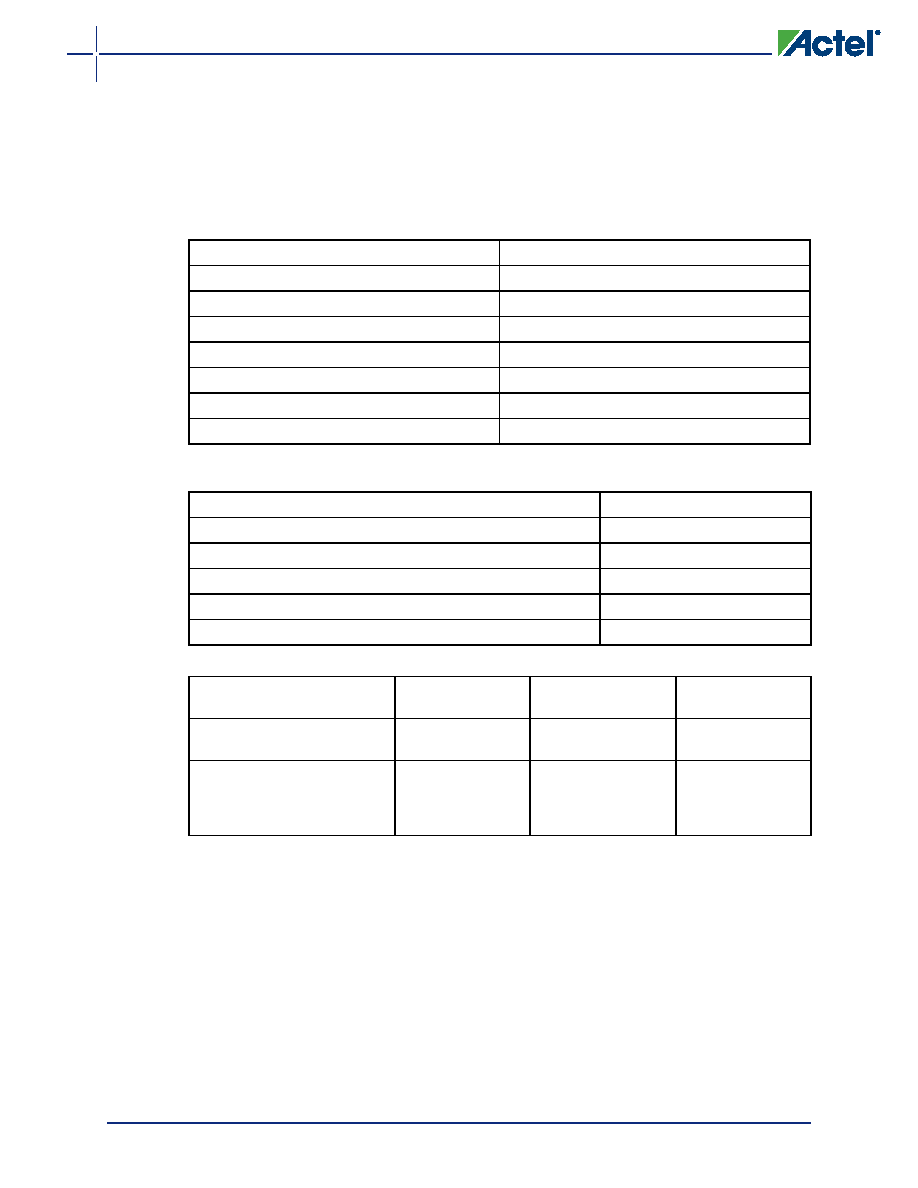
Table 2-31 Duration of Short Circuit Event before Failure
Temperature
Time before Failure
–40°C
> 20 years
–20°C
> 20 years
0°C
> 20 years
25°C
> 20 years
70°C
5 years
85°C
2 years
100°C
6 months
Table 2-32 Schmitt Trigger Input Hysteresis
Hysteresis Voltage Value (Typ.) for Schmitt Mode Input Buffers
Input Buffer Configuration
Hysteresis Value (typ.)
3.3 V LVTTL / LVCMOS (Schmitt trigger mode)
240 mV
2.5 V LVCMOS (Schmitt trigger mode)
140 mV
1.8 V LVCMOS (Schmitt trigger mode)
80 mV
1.5 V LVCMOS (Schmitt trigger mode)
60 mV
1.2 V LVCMOS (Schmitt trigger mode)
40 mV
Table 2-33 I/O Input Rise Time, Fall Time, and Related I/O Reliability
Input Buffer
Input Rise/Fall
Time (min.)
Input Rise/Fall Time
(max.)
Reliability
LVTTL/LVCMOS (Schmitt trigger
disabled)
No requirement
10 ns *
20 years (100°C)
LVTTL/LVCMOS (Schmitt trigger
enabled)
No requirement
No requirement, but
input noise voltage
cannot exceed Schmitt
hysteresis.
20 years (100°C)
* The maximum input rise/fall time is related to the noise induced into the input buffer trace. If the noise is
low, then the rise time and fall time of input buffers can be increased beyond the maximum value. The
longer the rise/fall times, the more susceptible the input signal is to the board noise. Actel recommends
signal integrity evaluation/characterization of the system to ensure that there is no excessive noise
coupling into input signals.
相关PDF资料 |
PDF描述 |
|---|---|
| AGLN250V2-ZCS81I | FPGA, 6144 CLBS, 250000 GATES, 250 MHz, PBGA81 |
| AGLN250V2-ZCS81 | FPGA, 6144 CLBS, 250000 GATES, 250 MHz, PBGA81 |
| AGLN030V2-ZCS81I | FPGA, 768 CLBS, 30000 GATES, 250 MHz, PBGA81 |
| AGLN030V2-ZCS81 | FPGA, 768 CLBS, 30000 GATES, 250 MHz, PBGA81 |
| AGLN030V2-ZQN48I | FPGA, 768 CLBS, 30000 GATES, 250 MHz, QCC48 |
相关代理商/技术参数 |
参数描述 |
|---|---|
| AGLN250V2-CSG81 | 功能描述:IC FPGA 250K 1.2-1.5V CSP81 RoHS:是 类别:集成电路 (IC) >> 嵌入式 - FPGA(现场可编程门阵列) 系列:IGLOO nano 标准包装:24 系列:ECP2 LAB/CLB数:1500 逻辑元件/单元数:12000 RAM 位总计:226304 输入/输出数:131 门数:- 电源电压:1.14 V ~ 1.26 V 安装类型:表面贴装 工作温度:0°C ~ 85°C 封装/外壳:208-BFQFP 供应商设备封装:208-PQFP(28x28) |
| AGLN250V2-CSG81I | 功能描述:IC FPGA NANO 1KB 250K 81-CSP RoHS:是 类别:集成电路 (IC) >> 嵌入式 - FPGA(现场可编程门阵列) 系列:IGLOO nano 标准包装:152 系列:IGLOO PLUS LAB/CLB数:- 逻辑元件/单元数:792 RAM 位总计:- 输入/输出数:120 门数:30000 电源电压:1.14 V ~ 1.575 V 安装类型:表面贴装 工作温度:-40°C ~ 85°C 封装/外壳:289-TFBGA,CSBGA 供应商设备封装:289-CSP(14x14) |
| AGLN250V2-DIELOT | 制造商:Microsemi Corporation 功能描述:AGLN250V2-DIELOT - Gel-pak, waffle pack, wafer, diced wafer on film 制造商:Microsemi SOC Products Group 功能描述:AGLN250V2-DIELOT - Gel-pak, waffle pack, wafer, diced wafer on film |
| AGLN250V2-QNG100I | 制造商:Microsemi Corporation 功能描述:FPGA IGLOO NANO FAMILY 250K GATES 130NM (CMOS) TECHNOLOGY 1. - Trays |
| AGLN250V2-VQ100 | 功能描述:IC FPGA NANO 1KB 250K 100VQFP RoHS:否 类别:集成电路 (IC) >> 嵌入式 - FPGA(现场可编程门阵列) 系列:IGLOO nano 标准包装:152 系列:IGLOO PLUS LAB/CLB数:- 逻辑元件/单元数:792 RAM 位总计:- 输入/输出数:120 门数:30000 电源电压:1.14 V ~ 1.575 V 安装类型:表面贴装 工作温度:-40°C ~ 85°C 封装/外壳:289-TFBGA,CSBGA 供应商设备封装:289-CSP(14x14) |
发布紧急采购,3分钟左右您将得到回复。