- 您现在的位置:买卖IC网 > PDF目录378403 > AN-136 (Integrated Device Technology, Inc.) A NEW GENERATION OF TAG SRAMS?THE IDT71215 AND PDF资料下载
参数资料
| 型号: | AN-136 |
| 厂商: | Integrated Device Technology, Inc. |
| 英文描述: | A NEW GENERATION OF TAG SRAMS?THE IDT71215 AND |
| 中文描述: | 作为TAG SRAM的呢?IDT71215和新一代 |
| 文件页数: | 2/12页 |
| 文件大小: | 103K |
| 代理商: | AN-136 |
2
A NEW GENERATION OF TAG SRAMS—THE IDT71215 AND IDT71216
APPLICATION NOTE AN-136
Integrated Tag RAMs operate as ordinary SRAMs, but
have an additional access mode in which a word of data (an
index) is internally read (but not driven off-chip) and compared
with the CPU address driven onto the Tag RAM’s data bus.
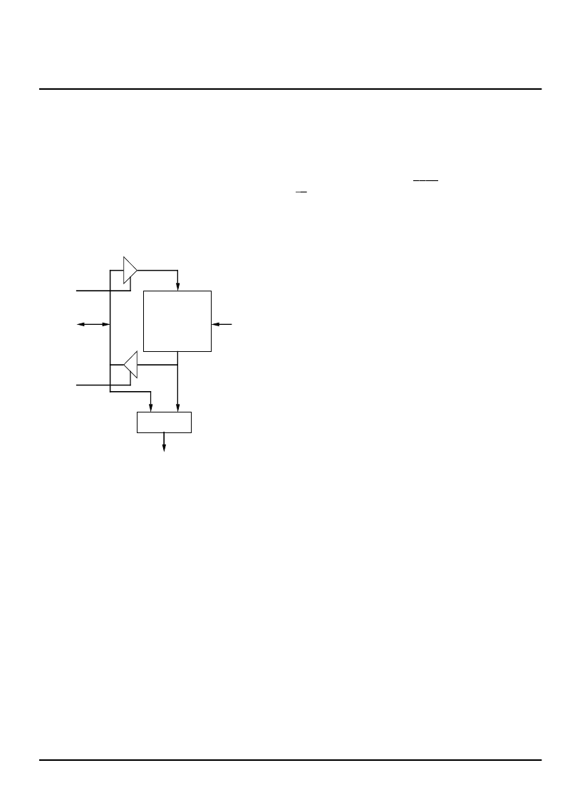
Figure 2 shows the basic architecture of an integrated Tag
SRAM. The comparator indicates whether the cache holds
the data for the address supplied by the CPU or other bus
master. This is a critical timing path since this tag “hit” or “miss”
must be determined before the cache memory access can be
completed (or even started, in many cases). Note that tag
memories connect only to the CPU address bus and never to
the CPU data bus.
BASIC TAG RAM ARCHITECTURE
DATA
IN
DATA
OUT
MEMORY
ADDRESS
DATA
(TAG)
WRITE
READ
COMPARE
MATCH
3176 drw 02
Figure 2. Basic Integrated Tag SRAM Architecture
An additional feature of the Tag SRAM is that a portion of
the memory is resettable. This permits use of one bit of the
data field as a “valid” status bit. Upon system initialization,
when the cache contains random data, a quick reset will clear
the valid bit for every cache line so that all initial cache
accesses will result in a miss. A miss then causes the address
to be loaded into the Tag RAM, data from main memory to be
loaded into the data RAMs, and the valid bit to be set true. If
not included in the Tag RAM, this function requires an addi-
tional 1-bit wide SRAM.
The reset feature of earlier Tag RAMs was sufficient for
implementation of a valid bit, but nothing more. Today’s
secondary caches frequently implement four-state write-back
protocols such as MESI, with multiprocessor applications
requiring five states (e.g. MOESI) or more. Hence, most
caches need a two- or three-bit status memory that is ac-
cessed separately from the tag memory. It is used in conjunc-
tion with the match output to determine the response to a CPU
memory access or a snoop. (A snoop is an operation initiated
by the system in order to maintain coherency between the
cache(s) and main memory.) This has typically been handled
with yet another RAM - a conventional separate I/O SRAM
organized as either x1 or x4. The 71215/16 includes a three-
bit status memory on chip.
THE 71215 AND 71216
As shown in Figure 3, these 16K x 15 RAMs are configured
internally as two memories: 16K x 12 for tag and 16K x 3 for
status. These two memories share the address bus but are
controlled independently. An important new feature is extra
pins and logic for generating
BRDY
(Intel’s Burst Ready) and
TA
(PowerPC’s Transfer Acknowledge). These are CPU input
signals which are time critical in zero wait state secondary
caches. I/O’s are 3.3V compatible and there is a low power
standby mode. All writes are synchronous as with burst data
SRAMs, while all reads and compares are asynchronous for
minimum delay. Two opposite polarity chip select pins are
provided for easy depth expansion.
相关PDF资料 |
PDF描述 |
|---|---|
| AN-242 | LJT 18C 18#20 SKT RECP |
| AN-40 | Application Note 40 |
| AN-5002 | LJT 18C 18#20 SKT WALL RECP |
| AN-5025 | Applications Using the GTLP10B320 |
| AN-5026 | Circular Connector; No. of Contacts:19; Series:MS27656; Body Material:Aluminum; Connecting Termination:Crimp; Connector Shell Size:15; Circular Contact Gender:Pin; Circular Shell Style:Wall Mount Receptacle; Insert Arrangement:15-19 RoHS Compliant: No |
相关代理商/技术参数 |
参数描述 |
|---|---|
| AN137 | 制造商:SILABS 制造商全称:SILABS 功能描述:LITHIUM ION BATTERY CHARGER USING C8051F300 |
| AN1375-521P | 制造商:未知厂家 制造商全称:未知厂家 功能描述:AN0625-521P |
| AN1393 | 制造商:PANASONIC 制造商全称:Panasonic Semiconductor 功能描述:Dual Comparators |
| AN1393(AN6914) | 制造商:PANASONIC 制造商全称:Panasonic Semiconductor 功能描述:Dual Comparators |
| AN1393S | 制造商:Panasonic Industrial Company 功能描述:IC |
发布紧急采购,3分钟左右您将得到回复。