参数资料
| 型号: | BR93L56RF-WE2 |
| 厂商: | Rohm Semiconductor |
| 文件页数: | 29/41页 |
| 文件大小: | 0K |
| 描述: | IC EEPROM 2KBIT 2MHZ 8SOP |
| 标准包装: | 1 |
| 格式 - 存储器: | EEPROMs - 串行 |
| 存储器类型: | EEPROM |
| 存储容量: | 2K (128 x 16) |
| 速度: | 2MHz |
| 接口: | Microwire 3 线串行 |
| 电源电压: | 1.8 V ~ 5.5 V |
| 工作温度: | -40°C ~ 85°C |
| 封装/外壳: | 8-SOIC(0.173",4.40mm 宽) |
| 供应商设备封装: | 8-SOP |
| 包装: | 标准包装 |
| 产品目录页面: | 1380 (CN2011-ZH PDF) |
| 其它名称: | BR93L56RF-WE2DKR |
第1页第2页第3页第4页第5页第6页第7页第8页第9页第10页第11页第12页第13页第14页第15页第16页第17页第18页第19页第20页第21页第22页第23页第24页第25页第26页第27页第28页当前第29页第30页第31页第32页第33页第34页第35页第36页第37页第38页第39页第40页第41页
�� �
�
�BR93L� -W� Series,� 93A� □□� -WM� Series,� BR93H� □□� -WC� Series�
�●� Timing� chart�
�Technical� Note�
�1)� Read� cycle� (READ)�
�~� ~�
�~� ~�
�~� ~�
�CS�
�*1�
�~� ~�
�SK�
�1�
�2�
�4�
�~� ~�
�n�
�n+1�
�~� ~�
�~� ~�
�BR93H56/66-WC� :� n=27,� m=7�
�DI�
�1�
�1�
�0�
�Am�
�~� ~�
�A1�
�A0�
�BR93H76/86-WC� :� n=29,� m=9�
�~� ~�
�*2�
�~� ~�
�DO�
�High-Z�
�~� ~�
�0�
�D15�
�D14�
�~� ~�
�D1�
�D0�
�D15� D14�
�~� ~�
�*2� The� following� address� data� output�
�(� auto� increment� function� )�
�*1� Start� bit�
�When� data� “1”� is� input� for� the� first� time� after� the� rise� of� CS,� this� is� recognized� as� a� start� bit.� And� when� “1”� is� input� after� plural� “0”� are� input,� it� is� recognized� as� a�
�start� bit,� and� the� following� operation� is� started.� This� is� common� to� all� the� commands� to� described� hereafter� .�
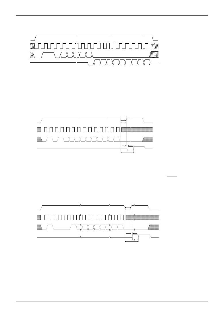
�Fig.� 30� Read� cycle�
�○� When� the� read� command� is� recognized,� input� address� data� (16bit)� is� output� to� serial.� And� at� that� moment,� at� taking� A0,� in�
�sync� with� the� rise� of� SK,� “0”� (dummy� bit)� is� output.� And,� the� following� data� is� output� in� sync� with� the� rise� of� SK.�
�This� IC� has� address� auto� increment� function� valid� only� at� read� command.� This� is� the� function� where� after� the� above� read�
�execution,� by� continuously� inputting� SK� clock,� the� above� address� data� is� read� sequentially.� And,� during� the� auto� increment,�
�keep� CS� at� “H”.�
�2)� Write� cycle� (WRITE)�
�CS�
�~~�
�~~�
�~~�
�~~�
�tCS�
�~~�
�~~�
�STATUS�
�SK�
�1�
�2�
�4�
�~~�
�~~�
�n�
�~~�
�BR93H56/66-WC� :� n=27,� m=7�
�BR93H76/86-WC� :� n=29,� m=9�
�DI�
�1�
�0�
�1�
�Am�
�~~�
�A1�
�A0�
�D15�
�D14�
�~~�
�D1�
�D0�
�~~�
�tSV�
�DO�
�High-Z�
�Fig.� 31� Write� cycle�
�BUSY�
�~~�
�tE/W�
�READY�
�In� this� command,� input� 16bit� data� (D15~D0)� are� written� to� designated� addresses� (Am~A0).� The� actual� write� starts� by� the� fall�
�of� CS� of� D0� taken� SK� clock(n-th� clock� from� the� start� bit� input),� to� the� rise� of� the� (n+1)-th� clock.�
�When� STATUS� is� not� detected,� (CS="L"� fixed)� Max.� 10ms(Max.5ms:BR93H66RFVM-WC)� in� conformity� with� tE/W,� and�
�when� STATUS� is� detected� (CS="H"),� all� commands� are� not� accepted� for� areas� where� "L"� (BUSY)� is� output� from� D0,�
�therefore,� do� not� input� any� command.�
�Write� is� not� made� even� if� CS� is� started� after� input� of� clock� after� (n+1)-th� clocks.�
�Note)� Take� tSKH� or� more� from� the� rise� of� the� n-th� clock� to� the� fall� of� CS.�
�3)� Write� all� cycyle� (WRAL)�
�CS�
�tCS�
�STATUS�
�SK�
�1�
�2�
�5�
�m�
�n�
�BR93H56/66-WC� :� n=27,� m=9�
�BR93H76/86-WC� :� n=29,� m=11�
�DI�
�1�
�0�
�0�
�0�
�1�
�B2�
�B1�
�B0�
�D15�
�D1�
�D0�
�tSV�
�DO�
�High-Z�
�Fig.� 32� Write� all� cycle�
�BUSY�
�tE/W�
�READY�
�In� this� command,� input� 16bit� data� is� written� simultaneously� to� designated� block� for� 128� words.� Data� is� writen� in� bulk� at� a�
�write� time� of� only� Max.� 10ms(Max.5ms:BR93H66RFVM-WC)� in� conformity� with� tE/W.� When� writing� data� to� all� addresses,�
�designate� each� block� by� B2,� B1,� and� B0,� and� execute� write.� Write� time� is� Max.10ms(Max.5ms:BR93H66RFVM-WC).� The�
�actual� write� starts� by� the� fall� of� CS� from� the� rise� of� D0� taken� at� SK� clock� (n-th� clock� from� the� start� bit� input),� to� the� rise� of� the�
�(n+1)-th� clock.� When� CS� is� ended� after� clock� input� after� the� rise� of� the� (n+1)-th� clock,� command� is� cancelled,� and� write� is�
�not� completed.�
�Note)Take� tSKH� or� more� from� the� rise� of� the� n-th� clock� to� the� fall� of� CS.�
�www.rohm.com�
�?� 2011� ROHM� Co.,� Ltd.� All� rights� reserved.�
�29/40�
�2011.09� -� Rev.G�
�相关PDF资料 |
PDF描述 |
|---|---|
| AGLN125V2-ZCSG81 | IC FPGA NANO 1KB 125K 81-CSP |
| A3PN250-VQ100 | IC FPGA NANO 250K GATES 100-VQFP |
| BR93L46RFJ-WE2 | IC EEPROM 1KBIT 2MHZ 8SOP |
| A3PN250-ZVQG100 | IC FPGA NANO 250K GATES 100-VQFP |
| A3PN250-ZVQ100 | IC FPGA NANO 250K GATES 100-VQFP |
相关代理商/技术参数 |
参数描述 |
|---|---|
| BR93L56-W | 功能描述:IC EEPROM 2KBIT 2MHZ 8DIP RoHS:是 类别:集成电路 (IC) >> 存储器 系列:- 标准包装:2,000 系列:- 格式 - 存储器:RAM 存储器类型:SRAM - 异步 存储容量:256K (32K x 8) 速度:15ns 接口:并联 电源电压:3 V ~ 3.6 V 工作温度:-40°C ~ 85°C 封装/外壳:28-TSSOP(0.465",11.8mm 宽) 供应商设备封装:28-TSOP 包装:带卷 (TR) 其它名称:71V256SA15PZGI8 |
| BR93L66 | 制造商:未知厂家 制造商全称:未知厂家 功能描述:EEPROM |
| BR93L66F | 制造商:未知厂家 制造商全称:未知厂家 功能描述:EEPROM |
| BR93L66FJ | 制造商:未知厂家 制造商全称:未知厂家 功能描述:EEPROM |
| BR93L66FJ-W | 制造商:ROHM 制造商全称:Rohm 功能描述:Microwire BUS 4Kbit(256 x 16bit) EEPROM |
发布紧急采购,3分钟左右您将得到回复。