- 您现在的位置:买卖IC网 > PDF目录223464 > BU-66318G0-110 (DATA DEVICE CORP) 2 CHANNEL(S), 1M bps, MIL-STD-1553 CONTROLLER, PQFP208 PDF资料下载
参数资料
| 型号: | BU-66318G0-110 |
| 厂商: | DATA DEVICE CORP |
| 元件分类: | 微控制器/微处理器 |
| 英文描述: | 2 CHANNEL(S), 1M bps, MIL-STD-1553 CONTROLLER, PQFP208 |
| 封装: | 28 X 28 MM, 1.40 MM HEIGHT, LQFP-208 |
| 文件页数: | 18/32页 |
| 文件大小: | 278K |
| 代理商: | BU-66318G0-110 |
第1页第2页第3页第4页第5页第6页第7页第8页第9页第10页第11页第12页第13页第14页第15页第16页第17页当前第18页第19页第20页第21页第22页第23页第24页第25页第26页第27页第28页第29页第30页第31页第32页
25
Data Device Corporation
www.ddc-web.com
BU-66318
B-09/05-0
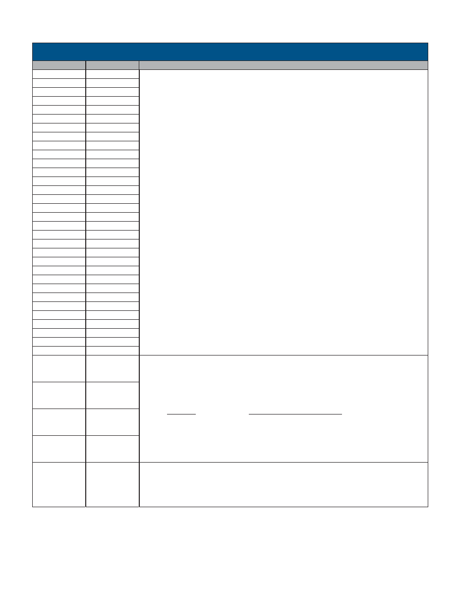
TABLE 27. PCI BUS ADDRESS AND DATA SIGNALS
SIGNAL NAME
PIN
DESCRIPTION
AD31 (MSB) (I/O)
12
AD30 (I/O)
14
AD29 (I/O)
16
AD28 (I/O)
17
AD27 (I/O)
18
AD26 (I/O)
19
AD25 (I/O)
22
AD24 (I/O)
23
AD23 (I/O)
26
AD22 (I/O)
32
AD21 (I/O)
36
AD20 (I/O)
43
AD19 (I/O)
45
AD18 (I/O)
46
AD17 (I/O)
62
AD16 (I/O)
63
32-Bit PCI Bus Address / Data lines. Address and Data are multiplexed on the same pins. Each bus opera-
tion consists of an address phase followed by one or more data phases.
Address phases are identified when the control signal FRAME# is asserted. Data transfers occur during
those clock cycles in which the control signals IRDY# and TRDY# are both asserted.
Bus Command and Byte Enables. These signals are multiplexed on the same pins. During the address
phase of a bus operation, these pins identify the bus command, as shown in the table of ACE-Bridge com-
mands below. During the data phase of a bus operation, these pins are used as Byte Enables, with
C/BE[0]# enabling byte 0 (LSB) and C/BE[3]# enabling byte 3 (MSB).
C/BE[3:0]#
Description (during address phase)
0
1
0
Memory Read
0
1
Memory Write
1
0
1
0
Configuration Read
1
0
1
Configuration Write
1
0
Memory Read - MULTIPLE
Parity. This signal is even parity across the entire AD[31:0] field along with the C/BE[3:0]# field. The parity
is stable in the clock following the address phase and is sourced by the Bus Master. During the data phase
for write operations, the Bus Master sources this signal on the clock following IRDY# active. During the
data phase for read operations, this signal is sourced by the Target and is valid on the clock following
TRDY# active. The PAR signal therefore has the same timing as AD[31:0], delayed by one clock.
AD15 (I/O)
64
AD14 (I/O)
65
AD13 (I/O)
85
AD12 (I/O)
87
AD11 (I/O)
92
AD10 (I/O)
94
AD9 (I/O)
95
AD8 (I/O)
111
AD7 (I/O)
114
AD6 (I/O)
115
AD5 (I/O)
121
AD4 (I/O)
147
AD3 (I/O)
165
AD2 (I/O)
166
AD1 (I/O)
167
AD0 (I/O) (LSB)
168
C/BE[3]# (I)
24
C/BE[2]# (I)
37
C/BE[1]# (I)
84
C/BE[0]# (I)
148
PAR(I/O)
35
相关PDF资料 |
PDF描述 |
|---|---|
| BU2294AF | 67.735842 MHz, OTHER CLOCK GENERATOR, PDSO8 |
| BU3076HFV-TR | 67.5 MHz, OTHER CLOCK GENERATOR, PDSO6 |
| BU6836 | PCMCIA BUS CONTROLLER, PBGA256 |
| BU7346GUL | 38 MHz, OTHER CLOCK GENERATOR, PBGA6 |
| BUF01900AIDRCR | SPECIALTY ANALOG CIRCUIT, PDSO10 |
相关代理商/技术参数 |
参数描述 |
|---|---|
| BU6650NUX | 制造商:ROHM 制造商全称:Rohm 功能描述:3ch CMOS LDO Regulators |
| BU6650NUX_11 | 制造商:ROHM 制造商全称:Rohm 功能描述:3ch CMOS LDO Regulators |
| BU6650NUX-TR | 功能描述:低压差稳压器 - LDO LDO REG 0.2A 8PIN 2.8V 2.8V 1.8V RoHS:否 制造商:Texas Instruments 最大输入电压:36 V 输出电压:1.4 V to 20.5 V 回动电压(最大值):307 mV 输出电流:1 A 负载调节:0.3 % 输出端数量: 输出类型:Fixed 最大工作温度:+ 125 C 安装风格:SMD/SMT 封装 / 箱体:VQFN-20 |
| BU6651NUX | 制造商:ROHM 制造商全称:Rohm 功能描述:High-speed Load Response Full CMOS LDP Regulators |
| BU6651NUX-TR | 功能描述:低压差稳压器 - LDO LDO REG 0.2A 8PIN 2.8V 1.8V 1.5V RoHS:否 制造商:Texas Instruments 最大输入电压:36 V 输出电压:1.4 V to 20.5 V 回动电压(最大值):307 mV 输出电流:1 A 负载调节:0.3 % 输出端数量: 输出类型:Fixed 最大工作温度:+ 125 C 安装风格:SMD/SMT 封装 / 箱体:VQFN-20 |
发布紧急采购,3分钟左右您将得到回复。