- 您现在的位置:买卖IC网 > PDF目录298892 > BX80524P300000 (INTEL CORP) 32-BIT, 300 MHz, MICROPROCESSOR, PPGA370 PDF资料下载
参数资料
| 型号: | BX80524P300000 |
| 厂商: | INTEL CORP |
| 元件分类: | 微控制器/微处理器 |
| 英文描述: | 32-BIT, 300 MHz, MICROPROCESSOR, PPGA370 |
| 封装: | 1.950 X 1.950 INCH, HEAT SINK, STAGGERED, PLASTIC, PGA-370 |
| 文件页数: | 17/88页 |
| 文件大小: | 1622K |
| 代理商: | BX80524P300000 |
第1页第2页第3页第4页第5页第6页第7页第8页第9页第10页第11页第12页第13页第14页第15页第16页当前第17页第18页第19页第20页第21页第22页第23页第24页第25页第26页第27页第28页第29页第30页第31页第32页第33页第34页第35页第36页第37页第38页第39页第40页第41页第42页第43页第44页第45页第46页第47页第48页第49页第50页第51页第52页第53页第54页第55页第56页第57页第58页第59页第60页第61页第62页第63页第64页第65页第66页第67页第68页第69页第70页第71页第72页第73页第74页第75页第76页第77页第78页第79页第80页第81页第82页第83页第84页第85页第86页第87页第88页
Intel Celeron Processor
24
Datasheet
NOTES:
1. Unless otherwise noted, all specifications in this table apply to all Intel
Celeron processor frequencies.
2. VTT must be held to 1.5 V ± 9%; dICC
1.5 V ± 3% while the Intel Celeron processor system bus is idle. This is measured at the processor edge
fingers.
3. VREF is generated on the processor substrate to be 2/3 VTT nominally with the S.E.P. package. It must be
created on the motherboard for processors in the PPGA package.
2.12
Intel Celeron Processor System Bus AC Specifications
The Intel Celeron processor system bus timings specified in this section are defined at the Intel
Celeron processor edge fingers and the processor core pads. Timings specified at the processor
edge fingers only apply to the S.E.P. Package and timings given at the processor core pads apply to
both the S.E.P. Package and the PPGA package. Unless otherwise specified, timings are tested at
the processor core during manufacturing. Timings at the processor edge fingers are specified by
design characterization. See Section 7.0 for the Intel Celeron processor signal definitions. Note
that at 66 MHz system bus operation, the Intel Celeron processor timings at the processor
edge fingers are identical to the Pentium II processor timings at the edge fingers. See the
Pentium
II Processor at 233, 266, 300, and 333 MHz (Order Number 243335) for more detail.
Table 20 cover TAP timing. For each pair of tables, the first table contains timing specifications for
measurement or simulation at the processor edge fingers. The second table contains specifications
for simulation at the processor core pads.
All Intel Celeron processor system bus AC specifications for the AGTL+ signal group are relative
to the rising edge of the BCLK input. All AGTL+ timings are referenced to VREF for both ‘0’ and
‘1’ logic levels unless otherwise specified.
The timings specified in this section should be used in conjunction with the I/O buffer models
provided by Intel. These I/O buffer models, which include package information, are available for
the Pentium II processor in Quad format as the Pentium II Processor I/O Buffer Models, Quad
XTK Format (Electronic Form). AGTL+ layout guidelines are also available in AP-585,
Pentium II Processor AGTL+ Guidelines (Order Number 243330).
Care should be taken to read all notes associated with a particular timing parameter.
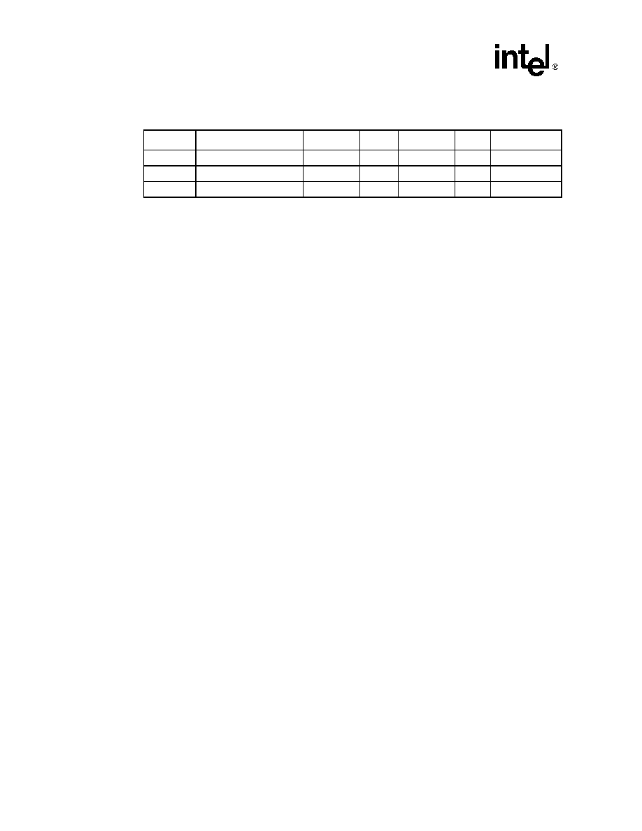
Table 7.
Intel Celeron Processor AGTL+ Bus Specifications 1
Symbol
Parameter
Min
Typ
Max
Units
Notes
VTT
Bus Termination Voltage
1.365
1.50
1.635
V
1.5 V ± 9% 2
RTT
Termination Resistor
56
± 5%
VREF
Bus Reference Voltage
2/
3 VTT
V
± 2% 3
相关PDF资料 |
PDF描述 |
|---|---|
| BX80525U500512E | 32-BIT, 500 MHz, MICROPROCESSOR, XMA |
| BX80525U533512E | 32-BIT, 533 MHz, MICROPROCESSOR, XMA |
| BX80525U550512E | 32-BIT, 550 MHz, MICROPROCESSOR, XMA |
| BX80525U450512E | 32-BIT, 450 MHz, MICROPROCESSOR, XMA |
| BX80526F500256E | 32-BIT, 500 MHz, MICROPROCESSOR, PPGA370 |
相关代理商/技术参数 |
参数描述 |
|---|---|
| BX80524R30012A | 制造商:未知厂家 制造商全称:未知厂家 功能描述:32-Bit Microprocessor |
| BX80524R33312A | 制造商:未知厂家 制造商全称:未知厂家 功能描述:32-Bit Microprocessor |
| BX80525U500256E | 制造商:未知厂家 制造商全称:未知厂家 功能描述:Microprocessor |
| BX80525U533256EB | 制造商:未知厂家 制造商全称:未知厂家 功能描述:Microprocessor |
| BX80525U550256E | 制造商:未知厂家 制造商全称:未知厂家 功能描述:Microprocessor |
发布紧急采购,3分钟左右您将得到回复。