- 您现在的位置:买卖IC网 > PDF目录17092 > C8051F300-TB (Silicon Laboratories Inc)BOARD PROTOTYPING W/C8051F300 PDF资料下载
参数资料
| 型号: | C8051F300-TB |
| 厂商: | Silicon Laboratories Inc |
| 文件页数: | 140/178页 |
| 文件大小: | 0K |
| 描述: | BOARD PROTOTYPING W/C8051F300 |
| 标准包装: | 1 |
| 类型: | MCU |
| 适用于相关产品: | C8051F300 |
| 所含物品: | 板 |
第1页第2页第3页第4页第5页第6页第7页第8页第9页第10页第11页第12页第13页第14页第15页第16页第17页第18页第19页第20页第21页第22页第23页第24页第25页第26页第27页第28页第29页第30页第31页第32页第33页第34页第35页第36页第37页第38页第39页第40页第41页第42页第43页第44页第45页第46页第47页第48页第49页第50页第51页第52页第53页第54页第55页第56页第57页第58页第59页第60页第61页第62页第63页第64页第65页第66页第67页第68页第69页第70页第71页第72页第73页第74页第75页第76页第77页第78页第79页第80页第81页第82页第83页第84页第85页第86页第87页第88页第89页第90页第91页第92页第93页第94页第95页第96页第97页第98页第99页第100页第101页第102页第103页第104页第105页第106页第107页第108页第109页第110页第111页第112页第113页第114页第115页第116页第117页第118页第119页第120页第121页第122页第123页第124页第125页第126页第127页第128页第129页第130页第131页第132页第133页第134页第135页第136页第137页第138页第139页当前第140页第141页第142页第143页第144页第145页第146页第147页第148页第149页第150页第151页第152页第153页第154页第155页第156页第157页第158页第159页第160页第161页第162页第163页第164页第165页第166页第167页第168页第169页第170页第171页第172页第173页第174页第175页第176页第177页第178页
C8051F300/1/2/3/4/5
64
Rev. 2.9
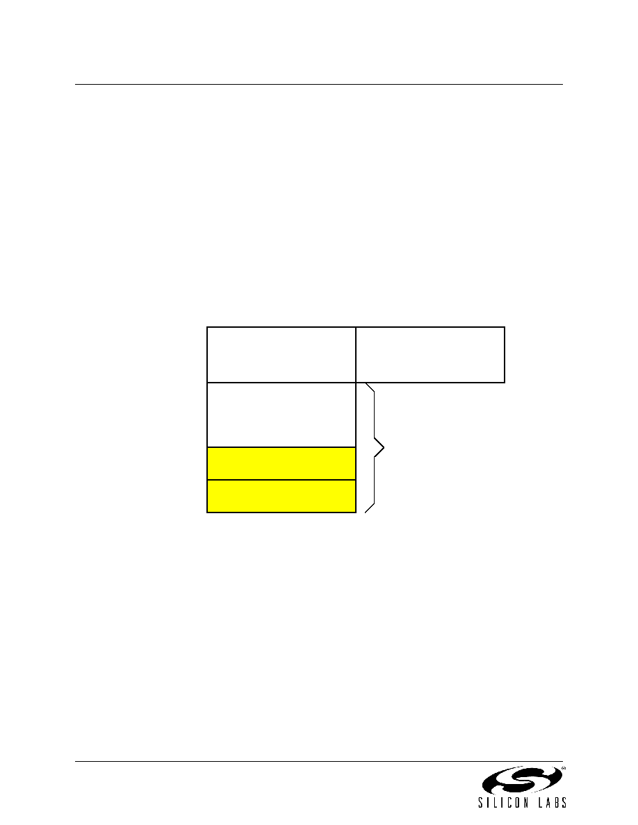
8.2.2. Data Memory
The CIP-51 includes 256 bytes of internal RAM mapped into the data memory space from 0x00 through
0xFF. The lower 128 bytes of data memory are used for general purpose registers and scratch pad mem-
ory. Either direct or indirect addressing may be used to access the lower 128 bytes of data memory. Loca-
tions 0x00 through 0x1F are addressable as four banks of general purpose registers, each bank consisting
of eight byte-wide registers. The next 16 bytes, locations 0x20 through 0x2F, may either be addressed as
bytes or as 128 bit locations accessible with the direct addressing mode.
The upper 128 bytes of data memory are accessible only by indirect addressing. This region occupies the
same address space as the Special Function Registers (SFR) but is physically separate from the SFR
space. The addressing mode used by an instruction when accessing locations above 0x7F determines
whether the CPU accesses the upper 128 bytes of data memory space or the SFRs. Instructions that use
direct addressing will access the SFR space. Instructions using indirect addressing above 0x7F access the
upper 128 bytes of data memory. Figure 8.3 illustrates the data memory organization of the CIP-51.
(Direct and Indirect
Addressing)
0x00
0x7F
Upper 128 RAM
(Indirect Addressing
Only)
0x80
0xFF
Special Function
Register's
(Direct Addressing Only)
General Purpose
Registers
0x1F
0x20
0x2F
Bit Addressable
Lower 128 RAM
(Direct and Indirect
Addressing)
0x30
INTERNAL DATA ADDRESS SPACE
Figure 8.3. Data Memory Map
8.2.3. General Purpose Registers
The lower 32 bytes of data memory, locations 0x00 through 0x1F, may be addressed as four banks of gen-
eral-purpose registers. Each bank consists of eight byte-wide registers designated R0 through R7. Only
one of these banks may be enabled at a time. Two bits in the program status word, RS0 (PSW.3) and RS1
(PSW.4), select the active register bank (see description of the PSW in SFR Definition 8.4). This allows
fast context switching when entering subroutines and interrupt service routines. Indirect addressing modes
use registers R0 and R1 as index registers.
相关PDF资料 |
PDF描述 |
|---|---|
| 0210391037 | CABLE JUMPER 1MM .102M 33POS |
| C8051F226-TB | BOARD PROTOTYPING W/C8051F226 |
| C8051F330-TB | BOARD PROTOTYPING W/C8051F330 |
| LGU2G101MELA | CAP ALUM 100UF 400V 20% SNAP |
| SDR-Q | SCOTCH CODE REFILL Q |
相关代理商/技术参数 |
参数描述 |
|---|---|
| C8051F300-TB-K | 功能描述:BOARD PROTOTYPING W/C8051F300 制造商:silicon labs 系列:- 零件状态:在售 板类型:评估平台 类型:MCU 8-位 核心处理器:8051 操作系统:- 平台:- 配套使用产品/相关产品:C8051F30x 安装类型:固定 内容:板 标准包装:1 |
| C8051F301 | 功能描述:8位微控制器 -MCU 8KB 2%osc RoHS:否 制造商:Silicon Labs 核心:8051 处理器系列:C8051F39x 数据总线宽度:8 bit 最大时钟频率:50 MHz 程序存储器大小:16 KB 数据 RAM 大小:1 KB 片上 ADC:Yes 工作电源电压:1.8 V to 3.6 V 工作温度范围:- 40 C to + 105 C 封装 / 箱体:QFN-20 安装风格:SMD/SMT |
| C8051F301-GM | 功能描述:8位微控制器 -MCU 8KB 11P MCU RoHS:否 制造商:Silicon Labs 核心:8051 处理器系列:C8051F39x 数据总线宽度:8 bit 最大时钟频率:50 MHz 程序存储器大小:16 KB 数据 RAM 大小:1 KB 片上 ADC:Yes 工作电源电压:1.8 V to 3.6 V 工作温度范围:- 40 C to + 105 C 封装 / 箱体:QFN-20 安装风格:SMD/SMT |
| C8051F301-GMR | 功能描述:8位微控制器 -MCU 8KB 11P MCU RoHS:否 制造商:Silicon Labs 核心:8051 处理器系列:C8051F39x 数据总线宽度:8 bit 最大时钟频率:50 MHz 程序存储器大小:16 KB 数据 RAM 大小:1 KB 片上 ADC:Yes 工作电源电压:1.8 V to 3.6 V 工作温度范围:- 40 C to + 105 C 封装 / 箱体:QFN-20 安装风格:SMD/SMT |
| C8051F301-GS | 功能描述:8位微控制器 -MCU 8KB Flash 2%osc RoHS:否 制造商:Silicon Labs 核心:8051 处理器系列:C8051F39x 数据总线宽度:8 bit 最大时钟频率:50 MHz 程序存储器大小:16 KB 数据 RAM 大小:1 KB 片上 ADC:Yes 工作电源电压:1.8 V to 3.6 V 工作温度范围:- 40 C to + 105 C 封装 / 箱体:QFN-20 安装风格:SMD/SMT |
发布紧急采购,3分钟左右您将得到回复。