- 您现在的位置:买卖IC网 > PDF目录17092 > C8051F300-TB (Silicon Laboratories Inc)BOARD PROTOTYPING W/C8051F300 PDF资料下载
参数资料
| 型号: | C8051F300-TB |
| 厂商: | Silicon Laboratories Inc |
| 文件页数: | 90/178页 |
| 文件大小: | 0K |
| 描述: | BOARD PROTOTYPING W/C8051F300 |
| 标准包装: | 1 |
| 类型: | MCU |
| 适用于相关产品: | C8051F300 |
| 所含物品: | 板 |
第1页第2页第3页第4页第5页第6页第7页第8页第9页第10页第11页第12页第13页第14页第15页第16页第17页第18页第19页第20页第21页第22页第23页第24页第25页第26页第27页第28页第29页第30页第31页第32页第33页第34页第35页第36页第37页第38页第39页第40页第41页第42页第43页第44页第45页第46页第47页第48页第49页第50页第51页第52页第53页第54页第55页第56页第57页第58页第59页第60页第61页第62页第63页第64页第65页第66页第67页第68页第69页第70页第71页第72页第73页第74页第75页第76页第77页第78页第79页第80页第81页第82页第83页第84页第85页第86页第87页第88页第89页当前第90页第91页第92页第93页第94页第95页第96页第97页第98页第99页第100页第101页第102页第103页第104页第105页第106页第107页第108页第109页第110页第111页第112页第113页第114页第115页第116页第117页第118页第119页第120页第121页第122页第123页第124页第125页第126页第127页第128页第129页第130页第131页第132页第133页第134页第135页第136页第137页第138页第139页第140页第141页第142页第143页第144页第145页第146页第147页第148页第149页第150页第151页第152页第153页第154页第155页第156页第157页第158页第159页第160页第161页第162页第163页第164页第165页第166页第167页第168页第169页第170页第171页第172页第173页第174页第175页第176页第177页第178页
Rev. 2.9
19
C8051F300/1/2/3/4/5
1.3.
On-Chip Debug Circuitry
The C8051F300/1/2/3/4/5 devices include on-chip Silicon Labs 2-Wire (C2) debug circuitry that provides
non-intrusive, full-speed, in-circuit debugging of the production part installed in the end application.
Silicon Labs' debugging system supports inspection and modification of memory and registers, break-
points, and single stepping. No additional target RAM, program memory, timers, or communications chan-
nels are required. All the digital and analog peripherals are functional and work correctly while debugging.
All the peripherals (except for the ADC and SMBus) are stalled when the MCU is halted, during single
stepping, or at a breakpoint in order to keep them synchronized.
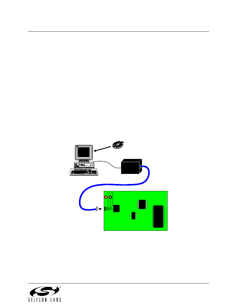
The C8051F300DK development kit provides all the hardware and software necessary to develop applica-
tion code and perform in-circuit debugging with the C8051F300/1/2/3/4/5 MCUs. The kit includes software
with a developer's studio and debugger, an integrated 8051 assembler, and a C2 debug adapter. It also
has a target application board with the associated MCU installed and large prototyping area, plus the nec-
essary communication cables and wall-mount power supply. The Development Kit requires a computer
with Windows 98 SE or later. The Silicon Labs IDE interface is a vastly superior developing and debug-
ging configuration, compared to standard MCU emulators that use onboard "ICE Chips" and require the
MCU in the application board to be socketed. Silicon Labs' debug paradigm increases ease of use and
preserves the performance of the precision analog peripherals.
Figure 1.6. Development/In-System Debug Diagram
1.4.
Programmable Digital I/O and Crossbar
C8051F300/1/2/3/4/5 devices include a byte-wide I/O Port that behaves like a typical 8051 Port with a few
enhancements. Each Port pin may be configured as an analog input or a digital I/O pin. Pins selected as
digital I/Os may additionally be configured for push-pull or open-drain output. The “weak pull-ups” that are
fixed on typical 8051 devices may be globally disabled, providing power savings capabilities.
TARGET PCB
RS-232
VDD
GND
C2 (x2), VDD, GND
WINDOWS 98 SE or Later
Silicon Labs Integrated
Development Environment
C8051F300
Debug
Adapter
相关PDF资料 |
PDF描述 |
|---|---|
| 0210391037 | CABLE JUMPER 1MM .102M 33POS |
| C8051F226-TB | BOARD PROTOTYPING W/C8051F226 |
| C8051F330-TB | BOARD PROTOTYPING W/C8051F330 |
| LGU2G101MELA | CAP ALUM 100UF 400V 20% SNAP |
| SDR-Q | SCOTCH CODE REFILL Q |
相关代理商/技术参数 |
参数描述 |
|---|---|
| C8051F300-TB-K | 功能描述:BOARD PROTOTYPING W/C8051F300 制造商:silicon labs 系列:- 零件状态:在售 板类型:评估平台 类型:MCU 8-位 核心处理器:8051 操作系统:- 平台:- 配套使用产品/相关产品:C8051F30x 安装类型:固定 内容:板 标准包装:1 |
| C8051F301 | 功能描述:8位微控制器 -MCU 8KB 2%osc RoHS:否 制造商:Silicon Labs 核心:8051 处理器系列:C8051F39x 数据总线宽度:8 bit 最大时钟频率:50 MHz 程序存储器大小:16 KB 数据 RAM 大小:1 KB 片上 ADC:Yes 工作电源电压:1.8 V to 3.6 V 工作温度范围:- 40 C to + 105 C 封装 / 箱体:QFN-20 安装风格:SMD/SMT |
| C8051F301-GM | 功能描述:8位微控制器 -MCU 8KB 11P MCU RoHS:否 制造商:Silicon Labs 核心:8051 处理器系列:C8051F39x 数据总线宽度:8 bit 最大时钟频率:50 MHz 程序存储器大小:16 KB 数据 RAM 大小:1 KB 片上 ADC:Yes 工作电源电压:1.8 V to 3.6 V 工作温度范围:- 40 C to + 105 C 封装 / 箱体:QFN-20 安装风格:SMD/SMT |
| C8051F301-GMR | 功能描述:8位微控制器 -MCU 8KB 11P MCU RoHS:否 制造商:Silicon Labs 核心:8051 处理器系列:C8051F39x 数据总线宽度:8 bit 最大时钟频率:50 MHz 程序存储器大小:16 KB 数据 RAM 大小:1 KB 片上 ADC:Yes 工作电源电压:1.8 V to 3.6 V 工作温度范围:- 40 C to + 105 C 封装 / 箱体:QFN-20 安装风格:SMD/SMT |
| C8051F301-GS | 功能描述:8位微控制器 -MCU 8KB Flash 2%osc RoHS:否 制造商:Silicon Labs 核心:8051 处理器系列:C8051F39x 数据总线宽度:8 bit 最大时钟频率:50 MHz 程序存储器大小:16 KB 数据 RAM 大小:1 KB 片上 ADC:Yes 工作电源电压:1.8 V to 3.6 V 工作温度范围:- 40 C to + 105 C 封装 / 箱体:QFN-20 安装风格:SMD/SMT |
发布紧急采购,3分钟左右您将得到回复。