- 您现在的位置:买卖IC网 > PDF目录17092 > C8051F300-TB (Silicon Laboratories Inc)BOARD PROTOTYPING W/C8051F300 PDF资料下载
参数资料
| 型号: | C8051F300-TB |
| 厂商: | Silicon Laboratories Inc |
| 文件页数: | 162/178页 |
| 文件大小: | 0K |
| 描述: | BOARD PROTOTYPING W/C8051F300 |
| 标准包装: | 1 |
| 类型: | MCU |
| 适用于相关产品: | C8051F300 |
| 所含物品: | 板 |
第1页第2页第3页第4页第5页第6页第7页第8页第9页第10页第11页第12页第13页第14页第15页第16页第17页第18页第19页第20页第21页第22页第23页第24页第25页第26页第27页第28页第29页第30页第31页第32页第33页第34页第35页第36页第37页第38页第39页第40页第41页第42页第43页第44页第45页第46页第47页第48页第49页第50页第51页第52页第53页第54页第55页第56页第57页第58页第59页第60页第61页第62页第63页第64页第65页第66页第67页第68页第69页第70页第71页第72页第73页第74页第75页第76页第77页第78页第79页第80页第81页第82页第83页第84页第85页第86页第87页第88页第89页第90页第91页第92页第93页第94页第95页第96页第97页第98页第99页第100页第101页第102页第103页第104页第105页第106页第107页第108页第109页第110页第111页第112页第113页第114页第115页第116页第117页第118页第119页第120页第121页第122页第123页第124页第125页第126页第127页第128页第129页第130页第131页第132页第133页第134页第135页第136页第137页第138页第139页第140页第141页第142页第143页第144页第145页第146页第147页第148页第149页第150页第151页第152页第153页第154页第155页第156页第157页第158页第159页第160页第161页当前第162页第163页第164页第165页第166页第167页第168页第169页第170页第171页第172页第173页第174页第175页第176页第177页第178页
C8051F300/1/2/3/4/5
84
Rev. 2.9
9.1.
Power-On Reset
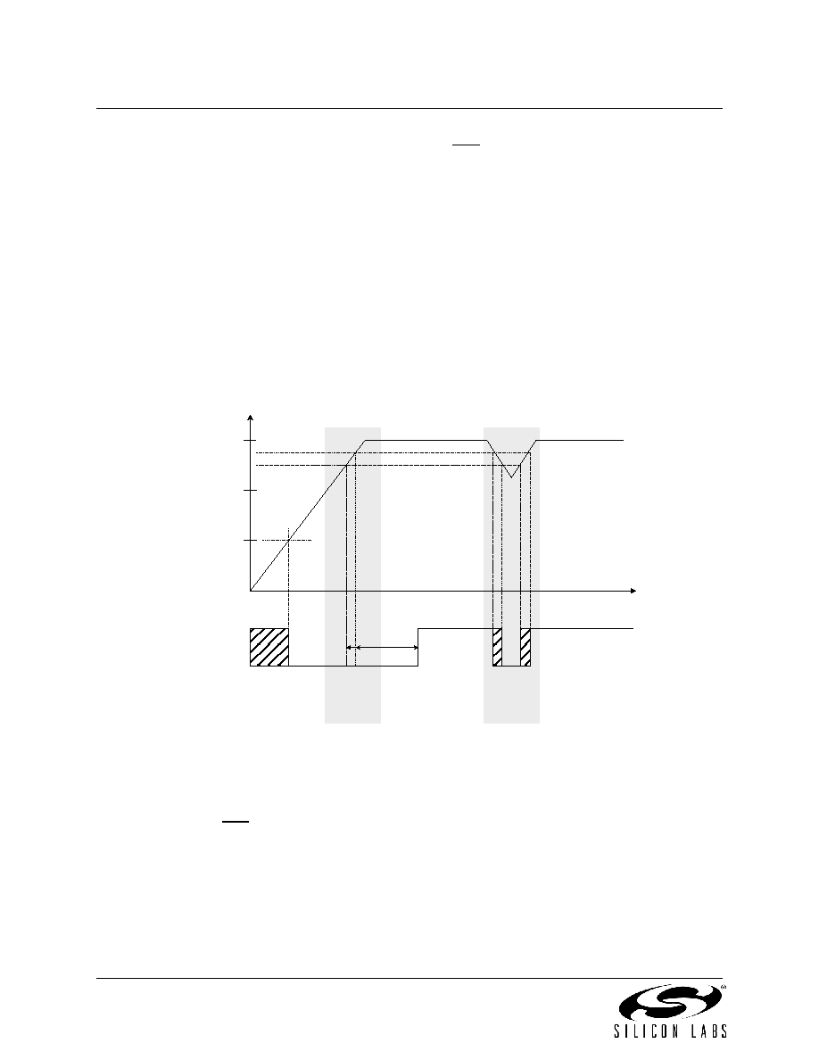
During powerup, the device is held in a reset state and the RST pin is driven low until VDD settles above
VRST. An additional delay occurs before the device is released from reset; the delay decreases as the VDD
ramp time increases (VDD ramp time is defined as how fast VDD ramps from 0 V to VRST). For valid ramp
times (less than 1 ms), the power-on reset delay (TPORDelay) is typically less than 0.3 ms.
Note: The maximum VDD ramp time is 1 ms; slower ramp times may cause the device to be
released from reset before VDD reaches the VRST level.
On exit from a power-on reset, the PORSF flag (RSTSRC.1) is set by hardware to logic 1. When PORSF is
set, all of the other reset flags in the RSTSRC Register are indeterminate (PORSF is cleared by all other
resets). Since all resets cause program execution to begin at the same location (0x0000) software can
read the PORSF flag to determine if a powerup was the cause of reset. The content of internal data mem-
ory should be assumed to be undefined after a power-on reset. The VDD monitor is disabled following a
power-on reset.
Power-On
Reset
VDD
Monitor
Reset
/RST
t
volt
s
1.0
2.0
Logic HIGH
Logic LOW
T
PORDelay
V
D
2.70
2.55
V
RST
VDD
Figure 9.2. Power-On and VDD Monitor Reset Timing
9.2.
Power-Fail Reset/VDD Monitor
When a power-down transition or power irregularity causes VDD to drop below VRST, the power supply
monitor will drive the RST pin low and hold the CIP-51 in a reset state (see Figure 9.2). When VDD returns
to a level above VRST, the CIP-51 will be released from the reset state. Note that even though internal data
memory contents are not altered by the power-fail reset, it is impossible to determine if VDD dropped below
the level required for data retention. If the PORSF flag reads ‘1’, the data may no longer be valid. The VDD
monitor is disabled after power-on resets; however its defined state (enabled/disabled) is not altered by
any other reset source. For example, if the VDD monitor is enabled and a software reset is performed, the
VDD monitor will still be enabled after the reset. The VDD monitor is enabled by writing a ‘1’ to the PORSF
相关PDF资料 |
PDF描述 |
|---|---|
| 0210391037 | CABLE JUMPER 1MM .102M 33POS |
| C8051F226-TB | BOARD PROTOTYPING W/C8051F226 |
| C8051F330-TB | BOARD PROTOTYPING W/C8051F330 |
| LGU2G101MELA | CAP ALUM 100UF 400V 20% SNAP |
| SDR-Q | SCOTCH CODE REFILL Q |
相关代理商/技术参数 |
参数描述 |
|---|---|
| C8051F300-TB-K | 功能描述:BOARD PROTOTYPING W/C8051F300 制造商:silicon labs 系列:- 零件状态:在售 板类型:评估平台 类型:MCU 8-位 核心处理器:8051 操作系统:- 平台:- 配套使用产品/相关产品:C8051F30x 安装类型:固定 内容:板 标准包装:1 |
| C8051F301 | 功能描述:8位微控制器 -MCU 8KB 2%osc RoHS:否 制造商:Silicon Labs 核心:8051 处理器系列:C8051F39x 数据总线宽度:8 bit 最大时钟频率:50 MHz 程序存储器大小:16 KB 数据 RAM 大小:1 KB 片上 ADC:Yes 工作电源电压:1.8 V to 3.6 V 工作温度范围:- 40 C to + 105 C 封装 / 箱体:QFN-20 安装风格:SMD/SMT |
| C8051F301-GM | 功能描述:8位微控制器 -MCU 8KB 11P MCU RoHS:否 制造商:Silicon Labs 核心:8051 处理器系列:C8051F39x 数据总线宽度:8 bit 最大时钟频率:50 MHz 程序存储器大小:16 KB 数据 RAM 大小:1 KB 片上 ADC:Yes 工作电源电压:1.8 V to 3.6 V 工作温度范围:- 40 C to + 105 C 封装 / 箱体:QFN-20 安装风格:SMD/SMT |
| C8051F301-GMR | 功能描述:8位微控制器 -MCU 8KB 11P MCU RoHS:否 制造商:Silicon Labs 核心:8051 处理器系列:C8051F39x 数据总线宽度:8 bit 最大时钟频率:50 MHz 程序存储器大小:16 KB 数据 RAM 大小:1 KB 片上 ADC:Yes 工作电源电压:1.8 V to 3.6 V 工作温度范围:- 40 C to + 105 C 封装 / 箱体:QFN-20 安装风格:SMD/SMT |
| C8051F301-GS | 功能描述:8位微控制器 -MCU 8KB Flash 2%osc RoHS:否 制造商:Silicon Labs 核心:8051 处理器系列:C8051F39x 数据总线宽度:8 bit 最大时钟频率:50 MHz 程序存储器大小:16 KB 数据 RAM 大小:1 KB 片上 ADC:Yes 工作电源电压:1.8 V to 3.6 V 工作温度范围:- 40 C to + 105 C 封装 / 箱体:QFN-20 安装风格:SMD/SMT |
发布紧急采购,3分钟左右您将得到回复。