- 您现在的位置:买卖IC网 > PDF目录366628 > C9832HT Up to 5A ULDO linear regulator PDF资料下载
参数资料
| 型号: | C9832HT |
| 英文描述: | Up to 5A ULDO linear regulator |
| 中文描述: | CPU系统时钟发生器|采用TSSOP | 56PIN |塑料 |
| 文件页数: | 3/24页 |
| 文件大小: | 169K |
| 代理商: | C9832HT |
C9832H
High Performance Pentium 4 Clock Synthesizer
Cypress Semiconductor Corporation
525 Los Coches St.
Milpitas, CA 95035. Tel: 408-263-6300, Fax: 408-263-6571
http://www.cypress.com
Document#: 38-07109 Rev. **
5/24/2001
Page 3 of 24
Approved Product
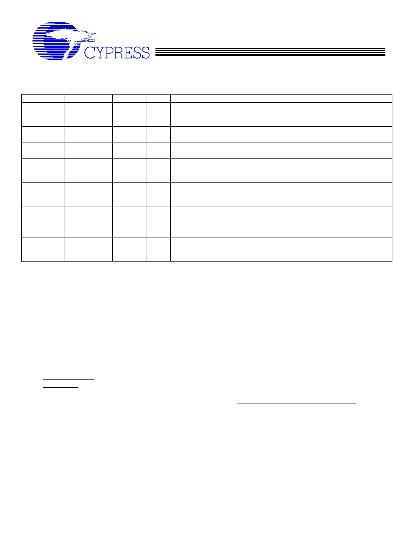
Pin Description (Cont.)
PIN
53
CPU_STP#
NAME
PWR
VDD
I/O
I
PU
Description
CPU Clock Disable Input. When asserted low, CPU (0:2) clocks are
synchronously disabled in a low state and CPU/(0:2) clocks are
synchronously disabled in an open state.
Input connection for 66CLK(0:2) output clock buffers if S2 = 1, or output
clock for fixed 66 MHz clock if S2=0. See table on page 1
3.3 volt clock outputs. These clocks are buffered copies of the 66IN
clock or fixed at 66 MHz. See table on page 1
3.3V Power Supply
24
66IN/3V66_5
VDD
I/O
21, 22, 23
66B(0:2)/
3V66(2:4)
VDD
VDD
O
1, 8, 14,
19, 32, 37,
46, 50
4, 9, 15,
20, 27, 31,
36, 47
41
PWR
VSS
PWR
Common Ground
VSSIREF
PWR
Current reference programming input for CPU buffers. A resistor is
connected between this pin and IREF. See CPU Clock current Select
Table in page 18 of this data sheet. This pin should also be returned to
device VSS.
Analog power input. Used for PLL and internal analog circuits. Is also
specifically used to detect and determine when power is at an
acceptable level to enable the device to operate.
26
VDDA
-
PWR
PU = Internal Pull-Up. PD = Internal Pull-Down. T = Tri level logic input with valid logic voltages of LOW=<0.8V, T=1.0-1.8V and
HIGH=>2.0V
2-Wire SMBus Control Interface
The 2-wire control interface implements a read/write slave only interface according to Philips I2C specification. (See
Application Note AN-0022).
The device will accept data written to the D2 address and data may read back from address D3. It will not respond to
any other addresses, and previously set control registers are retained as long as power in maintained on the device.
Serial Control Registers
Following the acknowledge of the Address Byte, two additional bytes must be sent:
1) “
Command Code
“
byte, and
2) “
Byte Count
” byte.
Although the data (bits) in the command is considered “don’t care”; it must be sent and will be acknowledged.
After the Command Code and the Byte Count have been acknowledged, the sequence (Byte 0, Byte 1, and Byte 2)
described below will be valid and acknowledged.
Note:
The Pin# column lists the relevant pin number where applicable. The @Pup column gives the default state at
power up.
相关PDF资料 |
PDF描述 |
|---|---|
| C9832HY | N-CHANNEL 60V - 0.014 Ohm - 60A TO-220/TO220FP STRIPFET POWER MOSFET |
| C9860-21 | 3 BAND EQUALIZER AUDIO PROCESSOR WITH SUBWOOFER CONTROL |
| C9860-22 | QUAD 2 CHANNEL MULTIPLEXER |
| C9860-23 | QUAD 2 CHANNEL MULTIPLEXER |
| C9860-24 | EXTERNALLY ADJUSTABLE MULTIFUNCTION REGULATOR |
相关代理商/技术参数 |
参数描述 |
|---|---|
| C9832HY | 制造商:未知厂家 制造商全称:未知厂家 功能描述:CPU SYSTEM CLOCK GENERATOR|SSOP|56PIN|PLASTIC |
| C98332-000 | 制造商:TE Connectivity 功能描述:QLL405 - Labels that come on sheets or rolls 制造商:TE Connectivity 功能描述:C98332-000 |
| C9835 | 制造商:CYPRESS 制造商全称:Cypress Semiconductor 功能描述:Low-EMI Clock Generator for Intel Mobile 133-MHz/3 SO-DIMM Chipset Systems |
| C9835CT | 制造商:CYPRESS 制造商全称:Cypress Semiconductor 功能描述:Low-EMI Clock Generator for Intel Mobile 133-MHz/3 SO-DIMM Chipset Systems |
| C9835CTT | 制造商:CYPRESS 制造商全称:Cypress Semiconductor 功能描述:Low-EMI Clock Generator for Intel Mobile 133-MHz/3 SO-DIMM Chipset Systems |
发布紧急采购,3分钟左右您将得到回复。